TR3002 查看數據表(PDF) - RF Monolithics, Inc
零件编号
产品描述 (功能)
生产厂家
TR3002 Datasheet PDF : 12 Pages
| |||
Pin
Name
Description
The PWIDTH pin sets the width of the ON pulse to the first RF amplifier tPW1 with a resistor RPW to ground (the ON pulse
width to the second RF amplifier tPW2 is set at 1.1 times the pulse width to the first RF amplifier). The ON pulse width tPW1
can be adjusted between 0.55 and 1 µs with a resistor value in the range of 200 K to 390 K. The value of RPW is given by:
RPW = 404* tPW1 - 18.6, where tPW1 is in µs and RPW is in kilohms
15
PWIDTH A ±5% resistor value is recommended. When this pin is connected to Vcc through a 1 M resistor, the RF amplifiers operate
at a nominal 50%-50% duty cycle, facilitating high data rate operation. In this case, the RF amplifier ON times are con-
trolled by the PRATE resistor as described above. It is important to keep the total capacitance between ground, Vcc and
this node to less than 5 pF to maintain stability. When using the high data rate operation with the sleep mode, connect the
1 M resistor between this pin and CNTRL1 (Pin 17), so this pin is low in the sleep mode.
VCC2 is the positive supply voltage pin for the receiver RF section and transmitter oscillator. Pin 16 must be bypassed with
16
VCC2
an RF capacitor, and must also be bypassed with a 1 to 10 µF tantalum or electrolytic capacitor. See the ASH Transceiver
Designer’s Guide for additional information.
CNTRL1 and CNTRL0 select the receive and transmit modes. CNTRL1 and CNTRL0 both high place the unit in the
receive mode. CNTRL1 high and CNTRL0 low place the unit in the ASK transmit mode. CNTRL1 low and CNTRL0 high
place the unit in the OOK transmit mode. CNTRL1 and CNTRL0 both low place the unit in the power-down (sleep) mode.
17
CNTRL1 CNTRL1 is a high-impedance input (CMOS compatible). An input voltage of 0 to 300 mV is interpreted as a logic low. An
input voltage of Vcc - 300 mV or greater is interpreted as a logic high. An input voltage greater than Vcc + 200 mV should
not be applied to this pin. A logic high requires a maximum source current of 40 µA. A logic low requires a maximum sink
current of 25 µA (1 µA in sleep mode). This pin must be held at a logic level; it cannot be left unconnected.
CNTRL0 is used with CNTRL1 to control the receive and transmit modes of the transceiver. CNTRL0 is a high-impedance
input (CMOS compatible). An input voltage of 0 to 300 mV is interpreted as a logic low. An input voltage of Vcc - 300 mV or
18
CNTRL0 greater is interpreted as a logic high. An input voltage greater than Vcc + 200 mV should not be applied to this pin. A logic
high requires a maximum source current of 40 µA. A logic low requires a maximum sink current of 25 µA (1 µA in sleep
mode). This pin must be held at a logic level; it cannot be left unconnected.
19
GND3
GND3 is an IC ground pin. It should be connected to GND1 by a short, low inductance trace.
RFIO is the RF input/output pin. This pin is connected directly to the SAW filter transducer. Antennas presenting an imped-
ance in the range of 35 to 72 ohms resistive can be satisfactorily matched to this pin with a series matching coil and a
20
RFIO
shunt matching/ESD protection coil. Other antenna impedances can be matched using two or three components. For
some impedances, two inductors and a capacitor will be required. A DC path from RFIO to ground is required for ESD pro-
tection.
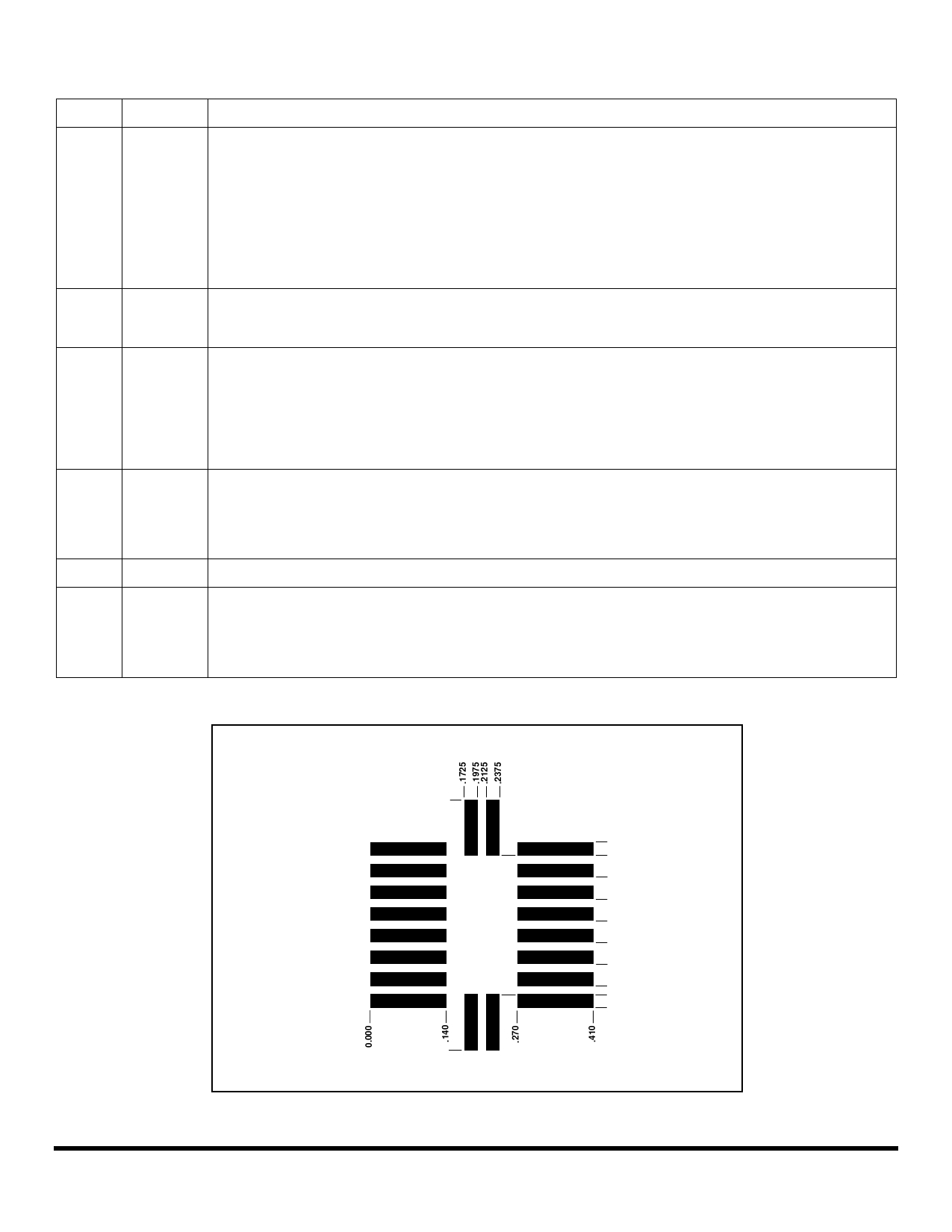
SM-20L PCB Pad Layout
.4600
0.000
Dimensions in inches
.3825
.3575
.3175
.2775
.2375
.1975
.1575
.1175
.1025
.0775
RF Monolithics, Inc. Phone: (972) 233-2903
Fax: (972) 387-8148
RFM Europe
Phone: 44 1963 251383
Fax: 44 1963 251510
©1999 by RF Monolithics, Inc. The stylized RFM logo are registered trademarks of RF Monolithics, Inc.
E-mail: info@rfm.com
http://www.rfm.com
TR3002-070605
Page 11 of 12
Share Link: 