TS1935 查看數據表(PDF) - TSC Corporation
零件编号
产品描述 (功能)
生产厂家
TS1935 Datasheet PDF : 8 Pages
| |||
TS1935
1.6MHz Boost Converter
with 30V Internal FET Switch
Absolute Maximum Rating
Parameter
Symbol
Limit
Input Voltage
VIN
6
EN, VFB Voltage
VEN, VFB
VIN
SW Voltage
VSW
30
Ambient Temperature Range
TA
-40 to +85
Junction Temperature Range
TJ
-40 to +125
Storage Temperature Range
TSTG
-65 to +150
ESD Classification
B*
Note: Stress above the listed absolute maximum rating may cause permanent damage to the device
* HBM B: 2000~3999V
Thermal Information
Parameter
Symbol
Thermal Resistance* (Junction to Case)
ӨJC
Thermal Resistance* (Junction to Ambient)
ӨJA
Internal Power Dissipation
PD
Maximum Junction Temperature
Solder Iron (10 Sec)**
* Measure ӨJC on center of molding compound if IC has no tab.
** MIL-STD-202G210F
Maximum
81
260
400
150
350
Pin Description
Pin Number Pin Name
1
SW
2
GND
3
FB
Description
Power Switch Input.
This is the drain of the internal NMOS power switch.
Minimize the metal trace area connected to this pin to minimize EMI.
Ground. Tie directly to ground plan.
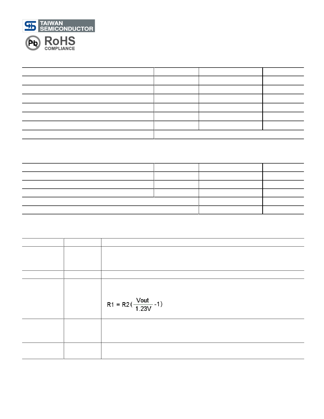
Output voltage feedback input.
Set the output voltage by selecting values for R1 and R2 using:
Unit
V
V
V
oC
oC
oC
Unit
oC/W
oC/W
mW
oC
oC
Connect the ground of the feedback network to a GND plane.
Enable, active high.
4
EN
The enable pin is an active high control. Tie this pin above 2V to enable the device.
Tie this pin below 0.4V to turn off the device.
Analog and Power input. Input Supply Pin.
5
IN
Place bypass capacitor as close to Vin as possible.
2/8
Version: A07
Share Link: 