TS7514 查看數據表(PDF) - STMicroelectronics
零件编号
产品描述 (功能)
生产厂家
TS7514 Datasheet PDF : 19 Pages
| |||
TS7514
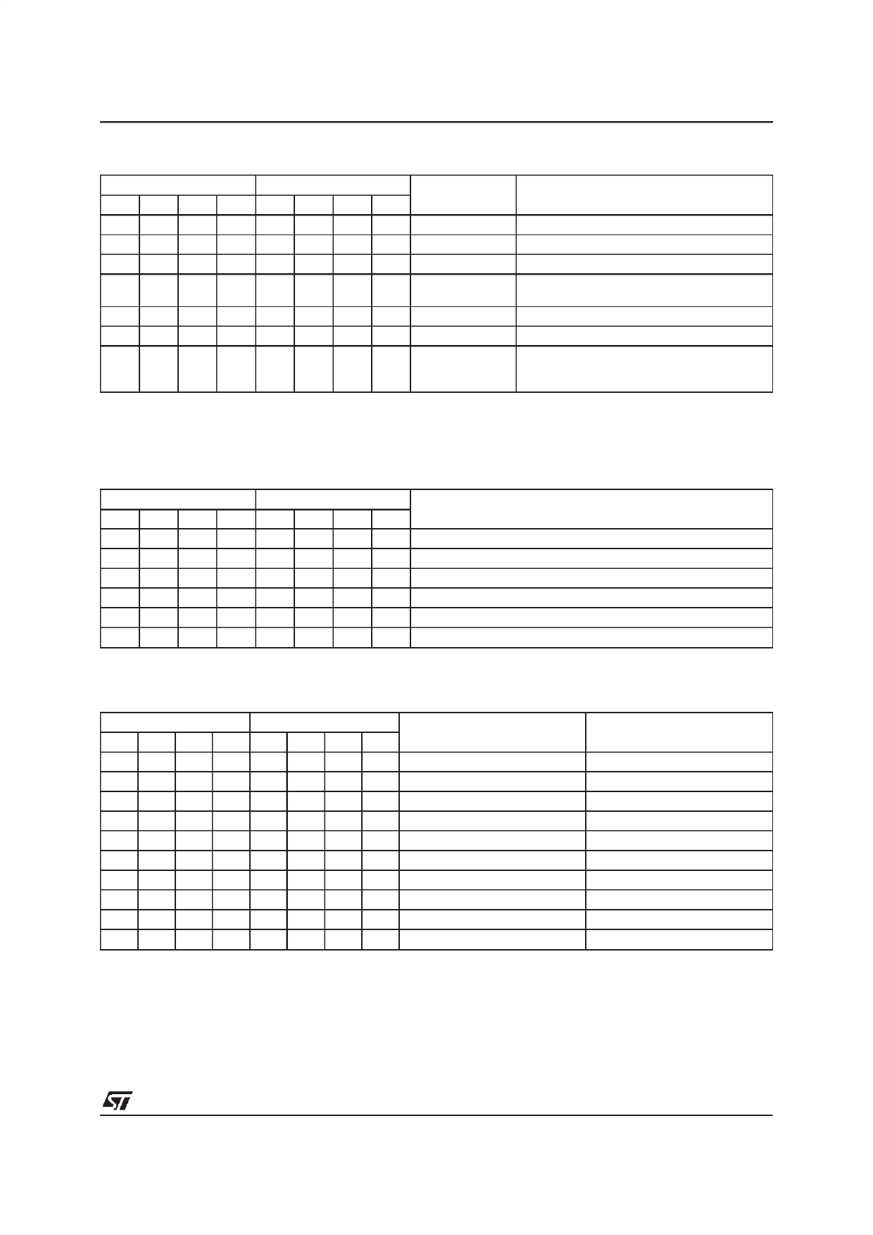
RECEIVE FILTER SELECTION AND GAIN PROGRAMMING REGISTER (RPRF REGISTER)
Address
Data
Reception Gain
D7 D6 D5 D4 D3 D2 D1 D0 (dB) (note 1)
Comments
P101XX00
0
XX01
+6*
XX10
+ 12
XX11
0
Rx Channel Band = Tx Channel B and Tx to
Rx Loopback – 33dBm ≤ Rx Level ≤ 40dBm
X 0 XX
X
Receive Filter Selected
X 1 XX
X
Receive Filter Desabled
1XXX
X
Receive F ilter Disconnected from RDI
Output and from Demodulator. Offset
Disabled.
* Power-up configuration.
Note 1 : Depending on the line length, the received signal can be amplified. Programmable reception gain allows a level close to +3dBm
at the filter input to take benefit of the maximum filter dynamic range (S/N ratio). The following requirement must be met :
max. line level + prog. gain ≤+3dBm.
TRANSMISSION FILTER PROGRAMMING REGISTER (RPTF REGISTER)
Address
Data
D7 D6 D5 D4 D3 D2 D1 D0
ATO Transmission
P 1 0 0 0 0 0 0 MODEM or DTMF Signal*
0 0 0 1 ATxI via Smoothing Filter and Attenuator
0 0 1 0 ATxI via Low-pass Filter and Attenuator
0 0 1 1 ATxI via Band-pass Filter and Attenuator
0 1 0 0 In DTMF Mode, Transmision of High Tone Frequency
1 0 0 0 In DTMF Mode, Transmission of Low Tone Frequency
* Power-up configuration.
HYSTERESIS AND SIGNAL DETECTION LEVEL PROGRAMMING REGISTER (RHDL REGISTER)
Address
Data
D7 D6 D5 D4 D3 D2 D1 D0
P11 0X0 0 0
X001
X010
X011
X100
X101
X110
X111
0XXX
1XXX
N2 (dBm) (note 1)
See Figu re 4
– 43 *
– 41
– 39
– 37
– 35
– 33
– 31
– 29
X
X
N1/N2 (dB)
X
X
X
X
X
X
X
X
3*
3.5
* Power-up configuration.
Note 1 : Detection low level measured at the demodulator input. The line signal detection level is obtained by reducing the gain ate the filter.
9/19
Share Link: 