MJD44H11(2011) 查看數據表(PDF) - ON Semiconductor
零件编号
产品描述 (功能)
生产厂家
MJD44H11 Datasheet PDF : 8 Pages
| |||
MJD44H11 (NPN)
MJD45H11 (PNP)
Complementary Power
Transistors
DPAK For Surface Mount Applications
Designed for general purpose power and switching such as output or
driver stages in applications such as switching regulators, converters,
and power amplifiers.
Features
• Lead Formed for Surface Mount Application in Plastic Sleeves
(No Suffix)
• Straight Lead Version in Plastic Sleeves (“−1” Suffix)
• Electrically Similar to Popular D44H/D45H Series
• Low Collector Emitter Saturation Voltage −
VCE(sat) = 1.0 Volt Max @ 8.0 Amperes
• Fast Switching Speeds
• Complementary Pairs Simplifies Designs
• Epoxy Meets UL 94 V−0 @ 0.125 in
• ESD Ratings: Human Body Model, 3B u 8000 V
Machine Model, C u 400 V
• These are Pb−Free Packages
MAXIMUM RATINGS
Rating
Collector−Emitter Voltage
Emitter−Base Voltage
Collector Current − Continuous
− Peak
Total Power Dissipation
@ TC = 25°C
Derate above 25°C
Total Power Dissipation (Note 1)
@ TA = 25°C
Derate above 25°C
Operating and Storage Junction
Temperature Range
Symbol
VCEO
VEB
IC
PD
PD
TJ, Tstg
Max
80
5
8
16
20
0.16
1.75
0.014
−55 to +150
Unit
Vdc
Vdc
Adc
W
W/°C
W
W/°C
°C
THERMAL CHARACTERISTICS
Characteristic
Symbol
Max
Unit
Thermal Resistance, Junction−to−Case
Thermal Resistance, Junction−to−Ambient
(Note 1)
RqJC
RqJA
6.25
°C/W
71.4
°C/W
Lead Temperature for Soldering
TL
260
°C
Stresses exceeding Maximum Ratings may damage the device. Maximum
Ratings are stress ratings only. Functional operation above the Recommended
Operating Conditions is not implied. Extended exposure to stresses above the
Recommended Operating Conditions may affect device reliability.
1. These ratings are applicable when surface mounted on the minimum pad
sizes recommended.
http://onsemi.com
SILICON
POWER TRANSISTORS
8 AMPERES
80 VOLTS, 20 WATTS
12
3
4
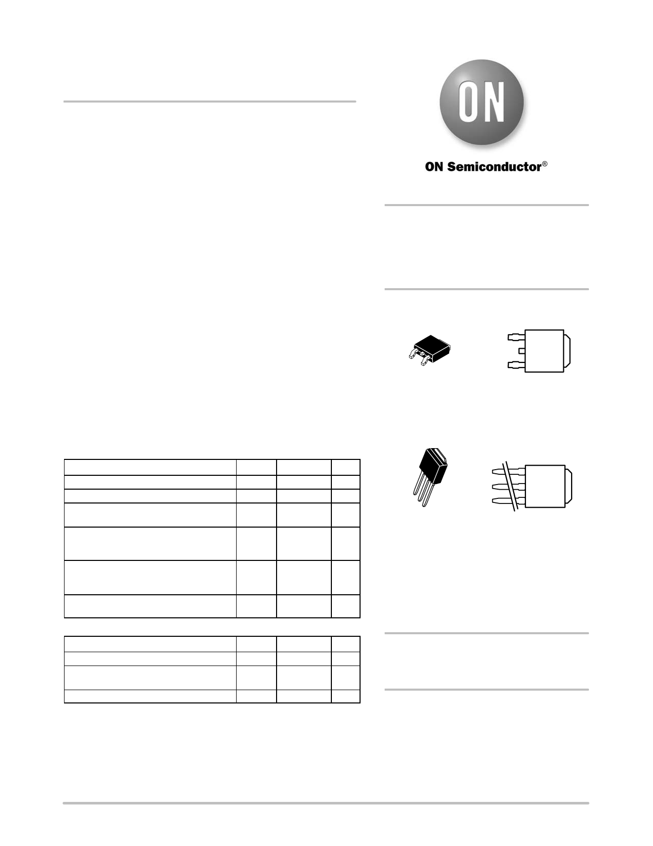
DPAK
CASE 369C
STYLE 1
MARKING
DIAGRAMS
AYWW
J4
xH11G
4
1
2
3
DPAK−3
CASE 369D
STYLE 1
AYWW
J4
xH11G
A
Y
WW
J4xH11
G
= Assembly Location
= Year
= Work Week
= Device Code
x = 4 or 5
= Pb−Free Package
ORDERING INFORMATION
See detailed ordering and shipping information in the package
dimensions section on page 6 of this data sheet.
© Semiconductor Components Industries, LLC, 2011
1
January, 2011 − Rev. 10
Publication Order Number:
MJD44H11/D
Share Link: 