AD9805 查看數據表(PDF) - Analog Devices
零件编号
产品描述 (功能)
生产厂家
AD9805 Datasheet PDF : 24 Pages
| |||
AD9807/AD9805
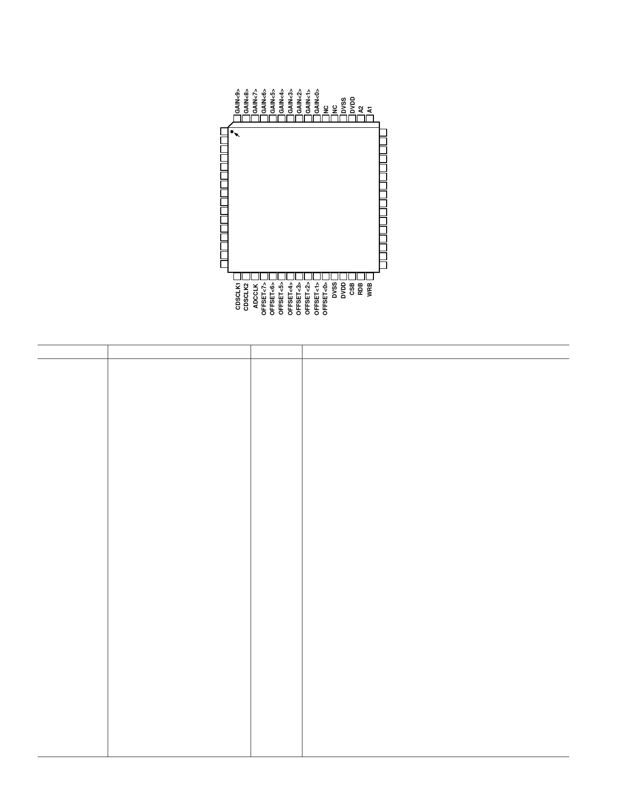
PIN CONFIGURATION
64 63 62 61 60 59 58 57 56 55 54 53 52 51 50 49
AVDD 1
AVSS 2
CAPT 3
CAPT 4
CAPB 5
CAPB 6
VREF 7
CML 8
VINR 9
AVSS 10
VING 11
AVSS 12
VINB 13
AVSS 14
AVDD 15
STRTLN 16
PIN 1
IDENTIFIER
AD9805
TOP VIEW
(Not to Scale)
48 A0
47 DOUT<9>
46 DOUT<8>
45 DOUT<7>
44 DOUT<6>
43 DOUT<5>/MPU<7>
42 DOUT<4>/MPU<6>
41 DRVDD
40 DRVSS
39 DOUT<3>/MPU<5>
38 DOUT<2>/MPU<4>
37 DOUT<1>/MPU<3>
36 DOUT<0>/MPU<2>
35 MPU<1>
34 MPU<0>
33 OEB
17 18 19 20 21 22 23 24 25 26 27 28 29 30 31 32
NC = NO CONNECT
PIN DESCRIPTIONS
Pin No.
Pin Name
Type
Description
1, 15
2, 10, 12, 14
3, 4
5, 6
7
8
9
11
13
16
17
18
19
28, 52
29, 51
20
21–26
27
30
31
32
33
34
35
36
37–39, 42
40
41
43
44–46
47
48, 49, 50
53, 54
55
56–63
64
AVDD
P
AVSS
P
CAPT
AO
CAPB
AO
VREF
AO
CML
AO
VINR
AI
VING
AI
VINB
AI
STRTLN
DI
CDSCLK1
DI
CDSCLK2
DI
ADCCLK
DI
DVSS
P
DVDD
P
OFFSET<7>
DI
OFFSET<6:1>
DI
OFFSET<0>
DI
CSB
DI
RDB
DI
WRB
DI
OEB
DI
MPU<0>
DIO
MPU<1>
DIO
DOUT<0>/MPU<2>
DIO
DOUT<1:4>/MPU<3:6>
DIO
DRVSS
P
DRVDD
P
DOUT<5>/MPU<7>
DIO
DOUT<6:8>
DO
DOUT<9>
DO
A0, A1, A2
DI
NC
GAIN<0>
DI
GAIN<1:8>
DI
GAIN<9>
DI
+5 V Analog Supply.
Analog Ground.
Reference Decoupling. See Figure 22.
Reference Decoupling.
Internal Reference Output. Decouple with 10 µF + 0.1 µF.
Internal Bias Voltage. Decouple with 0.1 µF.
Analog Input, Red.
Analog Input, Green.
Analog Input, Blue.
STRTLN. Indicates beginning of scan line.
CDS Reset Clock Pulse Input.
CDS Data Clock Pulse Input.
A/D Sample Clock Input.
Digital Ground.
+5 V Digital Supply.
Pixel Rate Offset Coefficient Inputs. Most Significant Bit.
Pixel Rate Offset Coefficient Inputs.
Pixel Rate Offset Coefficient Inputs. Least Significant Bit.
Chip Select. Active Low.
Read Strobe. Active Low.
Write Strobe. Active Low.
Output Enable. Active Low.
Register Input-Output LSB.
Register Input-Output.
Data Output LSB/Register Input-Output.
Data Output/Register Input-Output.
Digital Driver Ground.
Digital Driver Supply.
Data Output/Register Input-Output MSB.
Data Outputs.
Data Output MSB.
Register Select Pins.
No Connection.
Pixel Rate Gain Coefficient Input LSB.
Pixel Rate Gain Coefficient Inputs.
Pixel Rate Gain Coefficient Input MSB.
TYPE: AI = Analog Input; AO = Analog Output; DI = Digital Input; DO = Digital Output; DIO = Digital Input/Output; P = Power.
–6–
REV. 0
Share Link: 