UPD16634A 查看數據表(PDF) - NEC => Renesas Technology
零件编号
产品描述 (功能)
生产厂家
UPD16634A Datasheet PDF : 20 Pages
| |||
µPD16634A
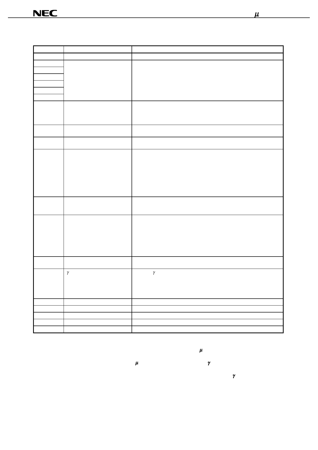
4. PIN FUNCTIONS
Pin Symbol
Pin Name
Description
S1 to S300
Driver output
The D/A converted 64-gray-scale analog voltage is output
D00 to D05
Display data input
The display data is input with a width of 36 bits, viz., the gray scale data
D10 to D15
(6 bits) by 6 dots (2 pixels).
D20 to D25
DX0 : LSB, DX5 : MSB
D30 to D35
D40 to D45
D50 to D55
R,/L
STHR
STHL
Shift direction switching input
Right shift start pulse
input/output
Left shift start pulse input/output
These refer to the start pulse input/output pins when cascades are
connected. The shift directions of the shift registers are as follows.
R,/L = H : STHR input, S1→S300, STHL output
R,/L = L : STHL input, S300→S1, STHR output
R,/L = H : Becomes the start pulse input pin.
R,/L = L : Becomes the start pulse output pin.
R,/L = H : Becomes the start pulse input pin.
R,/L = L : Becomes the start pulse output pin.
CLK
Shift clock input
Refers to the shift register’s shift clock input. The display data is
incorporated into the data register at the rising edge. At the rising edge of
the 50th clock after the start pulse input, the start pulse output reaches the
high level, thus becoming the start pulse of the next-level driver. The initial-
level driver’s 50th clock becomes valid as the next-level driver’s start pulse
is input. If 52 clock pulses are input after input of the start pulse, input of
display data is halted automatically. The contents of the shift register are
cleared at the STB’s rising edge.
STB
POL
Latch input
Polarity input
The contents of the data register are transferred to the latch at the rising
edge. And, at the falling edge, the gray scale voltage is supplied to the
driver. It is necessary to ensure input of one pulse per horizontal period.
POL = L ; The S2n-1 output uses V0 to V4 as the reference supply; and the S2n
output uses V5 to V9 as the reference supply.
POL = H ; The S2n-1 output uses V5 to V9 as the reference supply; and the
S2n output uses V0 to V4 as the reference supply.
S2n-1 indicates the odd output; and S2n indicates the even output. Input of
the POL signal is allowed the setup time (tPOL-STB) with respect to STB’s
rising edge.
POL2
V0 to V9
Data inversion input
γ-corrected power supplies
TEST
Test pin
POL2 = H : Display data is inverted.
POL2 = L : Display data is not inverted.
Input the γ-corrected power supplies from outside by using operational
amplifier. Make sure to maintain the following relationships. During the gray
scale voltage output, be sure to keep the gray scale level power supply at a
constant level.
VDD2 > V0 > V1 > V2 > V3 > V4 > V5 > V6 > V7 > V8 > V9 > VSS2
Set it to open.
VDD1
Logic circuit power supply
3.3 V ± 0.3 V
VDD2
Driver circuit power supply
8.0 V ± 0.5 V
VSS1
Logic ground
Grounding
VSS2
Driver ground
Grounding
Cautions 1. The power start sequence must be VDD1, logic input, and VDD2 & V0 to V9 in that order. Reverse
this sequence to shut down.(Simultaneous power application to VDD2 and V0 to V9 is possible.)
2. To stabilize the supply voltage, please be sure to insert 0.1 µF bypass capacitor between
VDD1-VSS1 and VDD2-VSS2. Furthermore, for increase precision of the D/A converter, insertion of a
bypass capacitor of about 0.01 µF is also advised between the γ-corrected power supply
terminals(V0,V1,V2...,V9) and VSS2.
3. We recommend to use Operational Amplifier to lower input impedance of γ-corrected voltage.
Data Sheet S12595EJ2V0DS00
5
Share Link: 