UPD16716N-XXX 查看數據表(PDF) - NEC => Renesas Technology
零件编号
产品描述 (功能)
生产厂家
UPD16716N-XXX
NEC => Renesas Technology

UPD16716N-XXX Datasheet PDF : 20 Pages
| |||
µ PD16716
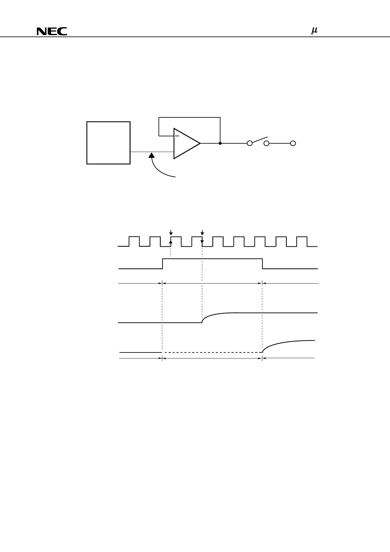
8. RELATIONSHIP BETWEEN STB, CLK, AND OUTPUT WAVEFORM
The output voltage is written to the LCD panel synchronized with the STB falling edge.
Figure 8−1. Output Circuit Block Diagram
DAC
Output AMP
+
VAMP(IN)
SW1
Sn
(VOUT)
Figure 8−2. Output Circuit Timing Waveform
CLK
(External Input)
STB
(External Input)
[1]
[2]
SW1 : ON
SW1 : OFF
SW1 : ON
VAMP(IN)
Sn
(VOUT:External Output)
Output
Hi-Z
Output
Remarks 1. STB = L : SW1 = ON
STB = H : SW1 = OFF
2. STB = “H” is acknowledged at timing [1].
3. The display data latch is completed at timing [2] and the input voltage
(VAMP(IN) : gray-scale level voltage) of the output amplifier changes.
10
Data Sheet S14417EJ1V1DS
Share Link: