UPD16716 查看數據表(PDF) - NEC => Renesas Technology
零件编号
产品描述 (功能)
生产厂家
UPD16716 Datasheet PDF : 20 Pages
| |||
µ PD16716
(2/2)
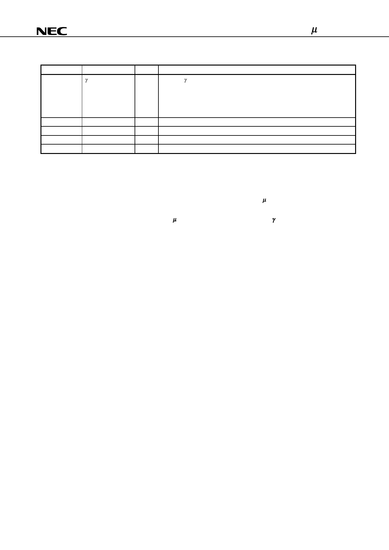
Pin Symbol
Pin Name
I/O
Description
V0 to V9
γ -corrected power
−
Input the γ -corrected power supplies from outside by using operational amplifier.
supplies
Make sure to maintain the following relationships. During the gray scale voltage
output, be sure to keep the gray scale level power supply at a constant level.
VDD2 – 0.1 V ≥ V0 > V1 > V2 > V3 > V4 ≥ 0.5 VDD2 ≥ V5 > V6 > V7 > V8 > V9 ≥ VSS2 +
0.1 V
VDD1
Logic power supply
−
2.5 V to 3.6 V
VDD2
Driver power supply
−
15.0 V ± 0.5 V
VSS1
Logic ground
−
Grounding
VSS2
Driver ground
−
Grounding
Cautions 1. The power start sequence must be VDD1, logic input, and VDD2 & V0 to V9 in that order.
Reverse this sequence to shut down. (Simultaneous power application to VDD2 and V0 to V9 is
possible.)
2. To stabilize the supply voltage, please be sure to insert a 0.1 µF bypass capacitor between
VDD1-VSS1 and VDD2-VSS2. Furthermore, for increased precision of the D/A converter, insertion of a
bypass capacitor of about 0.01 µF is also advised between the γ -corrected power supply
terminals (V0, V1, V2, ···, V9) and VSS2.
Data Sheet S14417EJ1V1DS
5
Share Link: 