UPD17201AGF 查看數據表(PDF) - NEC => Renesas Technology
零件编号
产品描述 (功能)
生产厂家
UPD17201AGF
NEC => Renesas Technology

UPD17201AGF Datasheet PDF : 120 Pages
| |||
µPD17201A, 17207
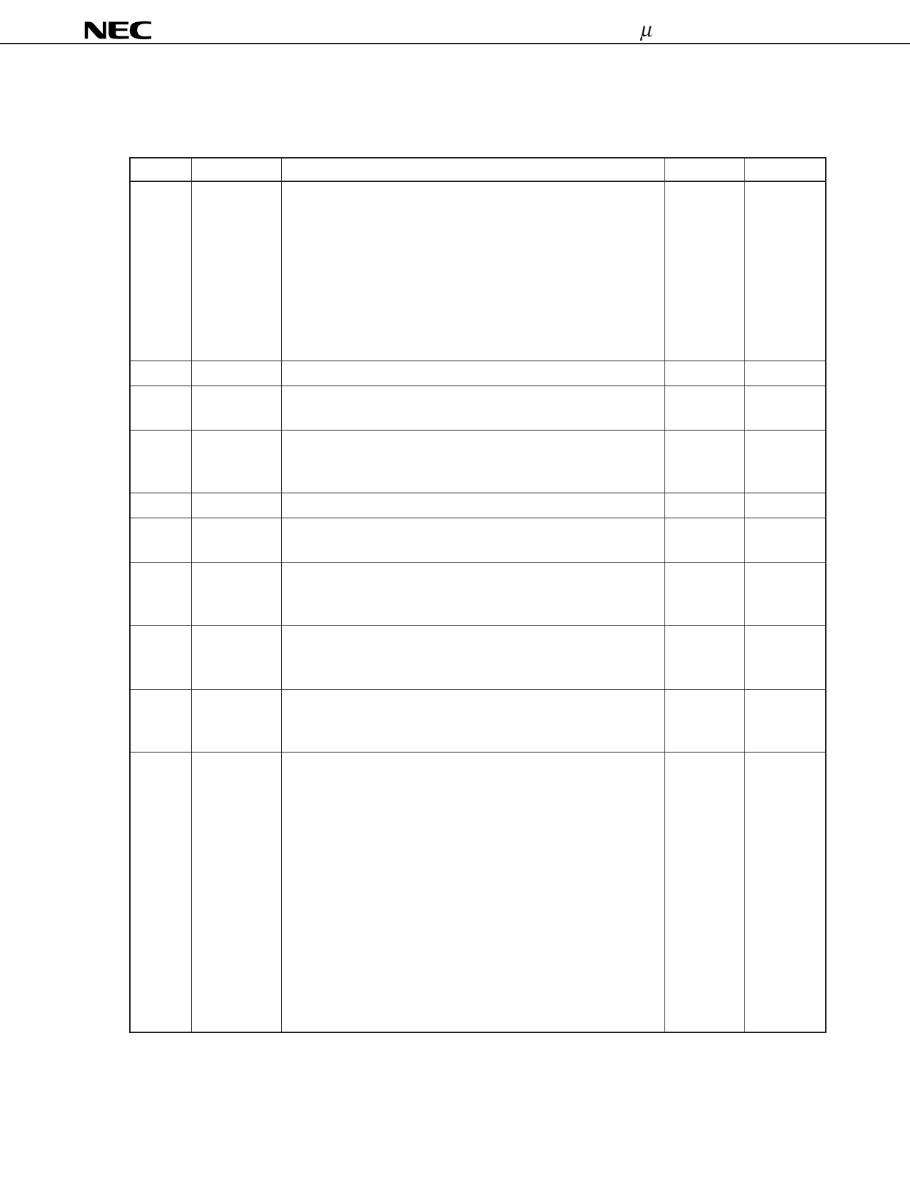
3. PINS FUNCTIONS
3.1 PIN IDENTIFICATION
Pin No.
76
77
78
79
80
1
|
32
34
33
35
36
|
39
40
41
42
|
45
46
|
49
50
|
53
54
55
56
57
Symbol
Function
Output Type
COM0
COM1
LCD35/COM2
LCD34/COM3
LCD33
LCD32
|
LCD1
LCD0
Common/segment signal outputs of the LCD driver. These
common and segment signal outputs are selected by LCDMD3 to
LCDMD0 of the register file.
• COM0 to COM3
• Common signal outputs of the LCD driver
• LCD35 to LCD0
• Segment signal outputs of the LCD driver
CMOS,
push-pull
GND
Device ground
–
VADC
Positive power supply of the A/D converter (VADC should be equal
–
to VDD.)
ADC0
Analog inputs of the A/D converter (8-bit resolution)
–
|
ADC3
GNDADC
Ground of the A/D converter
–
INT
External interrupt request signal (Input).
–
The interrupt request is generated at the rising edge of this signal.
P0A0
|
P0A3
4-bit I/O port (enabling setting of inputs or outputs in 4-bit units)
(Grouped I/O).
Each of these pins has a pull-up resistor.
CMOS,
push-pull
P0B0
|
P0B3
4-bit I/O port (enabling setting of inputs or outputs in 4-bit units).
(Grouped I/O).
N-channel,
open-drain
P0C0
|
P0C3
4-bit I/O port (enabling setting of inputs or outputs in 4-bit units).
(Grouped I/O).
N-channel,
open-drain
P0D0/LED
P0D1/TMOUT
P0D2
P0D3
Port 0D/LED output or port 0D/8-bit timer output.
P0D0 and LED outputs are switched by NRZEN of the register file.
P0D1 and 8-bit timer outputs are switched by TMOE of the register
file.
• P0D0 to P0D3
• 4-bit I/O port
• Enabling setting of inputs or outputs of each bit (Bitwise I/O)
• LED
• Outputs NRZ signal in synchronization with infrared remote
controller signal (REM)
• Outputs high level while remote controller carrier is output
from REM pin
• TMOUT
• Output of the 8-bit timer
CMOS,
push-pull
On Reset
–
–
–
–
–
Input
Input
Input
Input
Input
(to be cont’d)
9
Share Link: