US1050 查看數據表(PDF) - Unisem
零件编号
产品描述 (功能)
生产厂家
US1050 Datasheet PDF : 7 Pages
| |||
US1050
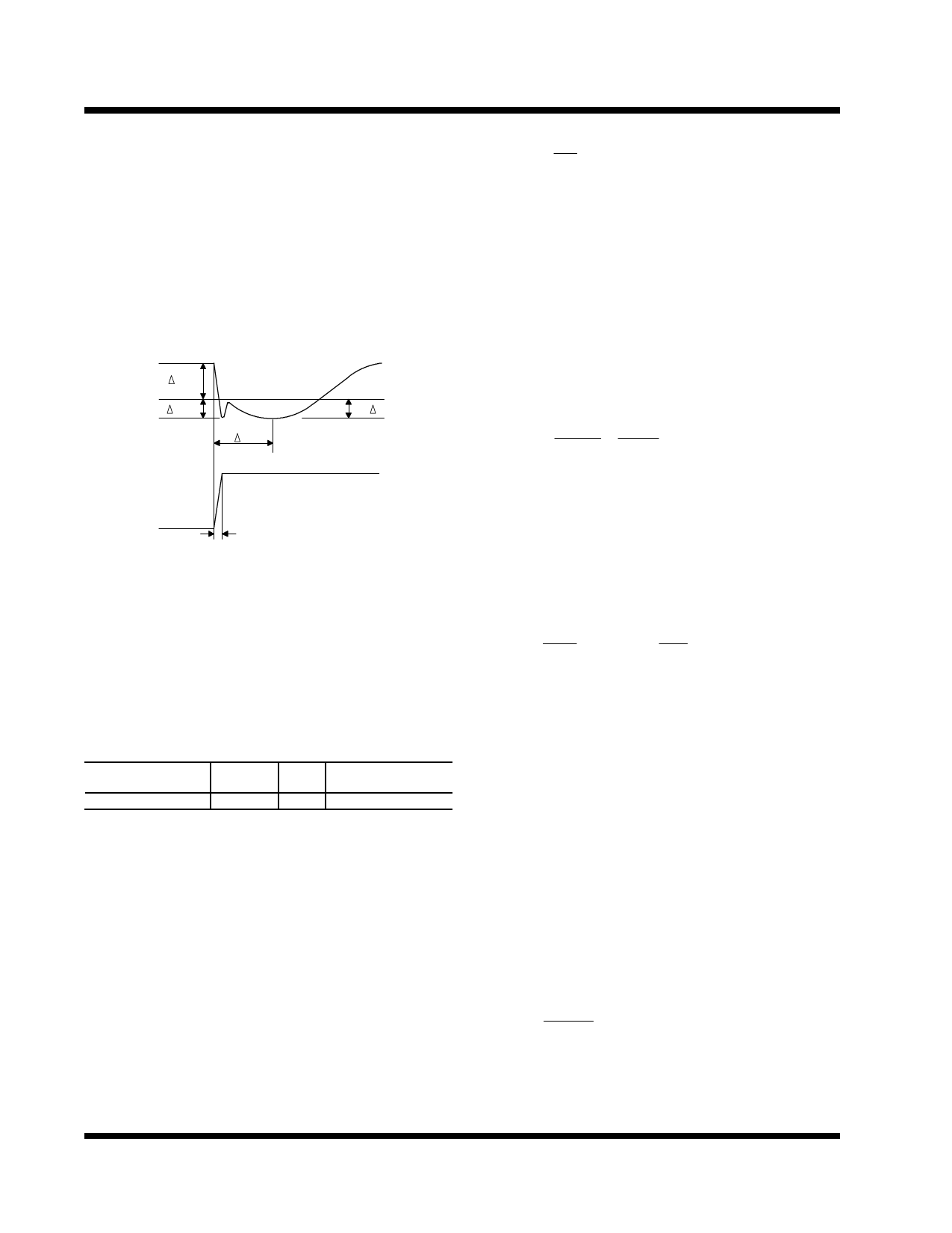
output voltage of the regulator. As shown in this figure,
the ESR of the output capacitor produces an instanta-
neous drop equalto the (∆VESR=ESR*∆I) and the ESL
effect will be equal to the rate of change of the output
current times the inductance of the capacitor. (∆VESL
=L*∆I/∆t) . The output capacitance effect is a droop in
the output voltage proportional to the time it takes for
the regulator to respond to the change in the current ,
(∆VC = ∆t * ∆I / C ) where ∆t is the response time of the
regulator.
ESR ≤ 37 =8 mΩ
4. 6
The Sanyo MVGX series is a good choice to achieve
both price and performance goals.The 6MV1500GX ,
1500uF, 6.3V has an ESR of less than 36 mΩ typ .
Selecting 5 of these capacitors in parallel has an ESR
of ≈7.2 mΩ which achieves our design goal.
The next step is to calculate the drop due to the capaci-
tance discharge and make sure that this drop in voltage
is less than the selected ESL drop in the previous step.
V ESR
V ESL
T
LOAD
CURRENT
VC
1050plt1-1.0
2) The output capacitance is 5X1500 uF = 7500uF
∆VC = ∆t × ∆I = 2×4.6 =1.2 mV
C 7500
Where :
∆t=2 uS is the regulator response time
LOAD CURRENT RISE TIME
To set the output DC voltage, we need to select R1 and
R2 :
Figure 4 - Typical Regulator response to the fast load
current step.
An example of a regulator design to meet the Intel
P54C™ VRE specification is given below .
3) Assuming R1=121 Ω , 0.1%
R2=
VOUT
VREF
−1
×121=
3.5
1.25
−1
×121=217.8
Ω
Select R2=218 Ω ,0.1%
Assume the specification for the processor as shown in
Table 1:
Type of
Processor
Intel-P54C VRE
Vout
Nominal
3.50 V
Imax
4.6 A
Max Allowed
Output Tolerance
±100 mV
Selecting both R1 and R2 resistors to be 0.1% toler-
ance, results in the least amount of error introduced by
the resistor dividers leaving ≈ ±1.3% error budget for
the US1050 reference which is within the initial accu-
racy of the device.
Table 1 - Processr Specification
The first step is to select the voltage step allowed in the
output due to the output capacitor’s ESR :
1) Assuming the regulator’s initial accuracy plus the re-
sistor divider tolerance is ≈ ±53 mV (±1.5% of 3.5V nomi-
nal) ,then the total step allowed for the ESR and the
ESL, is −47 mV .
Assuming that the ESL drop is −10mV ,the remaining
ESR step will be −37 mV . Therefore the output capaci-
tor ESR must be :
Finally , the input capacitor is selected as follows :
4) Assuming that the input voltage can drop 150mV be-
fore the main power supply responds, and that the main
power supply response time is ≈ 50 uSec, then the mini-
mum input capacitance for a 4.6A load step is given by
CIN = 4.6×50 =1530 µF
0.15
2-38
Rev. 1.3
10/27/00
Share Link: 