VCC6-D 查看數據表(PDF) - Vectron International
零件编号
产品描述 (功能)
生产厂家
VCC6-D Datasheet PDF : 7 Pages
| |||
VCC6-D, Dual Rate 106.250/212.500 LVPECL or LVDS XO
Performance Characteristics
Table 1. Electrical Performance
Parameter
Symbol
Min
Typical Max Units
Frequency
Supply Voltage 1
Supply Current, PECL
LVDS
fO
106.250 / 212.500
MHz
VDD
3.0
3.6
V
IDD
50
65
mA
53
67
Output Logic Levels, 0/70°C
PECL Output Logic High2
PECL Output Logic Low2
LVDS Output High Voltage
VOH
VDD-1.025
VOL
VOH
V
VDD-1.620 V
1.475
V
LVDS Output Low Voltage
LVDS Differential Output Voltage
VOL
|VOD|
0.925
250
V
400
mV
LVDS Change in Magnitude
LVDS Offset Output Voltage
delta|VOD|
VOS
1.125
25
mV
1.275
V
LVDS Change in Magnitude of Output Offset delta|VOS|
Transition Times
Rise Time2
tR
Fall Time2
tF
Symmetry or Duty Cycle3
SYM
45
25
mV
600
ps
600
ps
50
55
%
Operating temperature
Stability (ordering option)4
-10/70
°C
+/-50 or +/-100
ppm
RMS Jitter, 12kHz to 20 MHz, fO<200MHz
0.75
pS
Cycle-Cycle Jitter, rms
4
pS
Output Enabled5 , Frequency Select
Output Disabled5, Frequency Select
Logic Input Current, High
VIH
2
VIL
IIH
-10
V
0.8
V
+10
uA
Logic Input Current, Low
Package Size
IIL
-50
+50
uA
5.0 x 7.5 x 1.8
mm
1. A 0.01uF and a 0.1uF capacitor should be located as close to the supply as possible (to ground) is recommended.
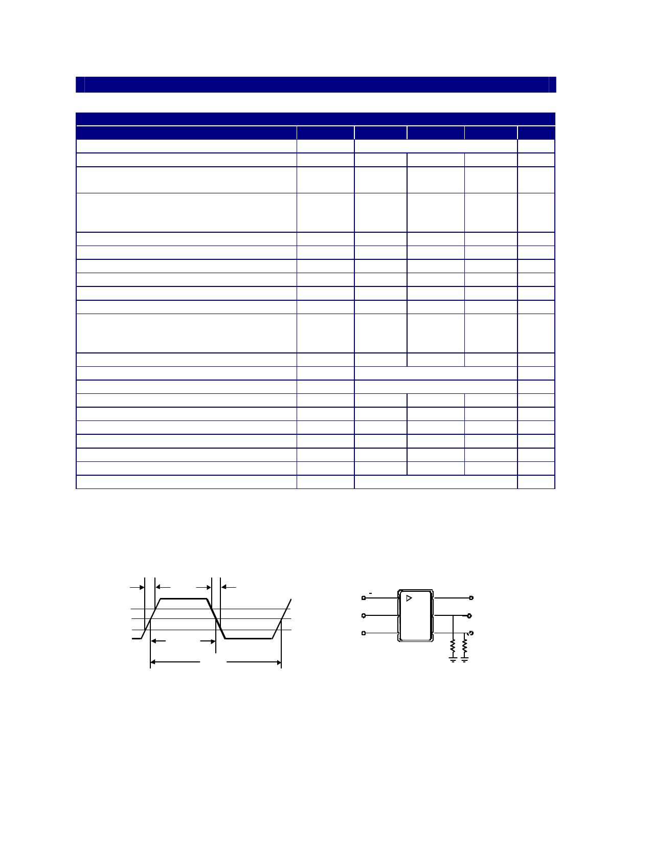
2. Figure 1 defines these parameters. Figure 2 illustrates the operating conditions under which
these parameters are tested and specified.
3. Symmetry is measured defined as Vs, On Time/Period.
4. Includes calibration tolerance, operating temperature, supply voltage variations, aging (40 degreesC/10 years) and shock and
vibration (not under operation). Aging budget is +/-5 ppm.
5. Output w ill be enabled if enable/disable is left open. Output frequency=106M250 if FREQ is left open.
80 %
Vs
20 %
tR
tF
On Time
Period
Figure 1. Output Waveform
(>0.975V, Open)
1
2
(-0.5V)
3
(+2V)
6
COutput
5
Output
4
50Ω
50Ω
Test Circuit Notes:
1) To Permit 50Ω Measurement of Outputs, all DC Inputs are Biased Down 0.5V.
2) All Voltage Sources Contain Bypass Capacitors to Minimize Supply Noise.
3) 50Ω Terminations are Within Test Equipment.
Figure 2. Typical Output Test Conditions (25±5°C)
Vectron International 267 Lowell Rd, Hudson NH 03051 Tel: 1-88-VECTRON-1 e-mail: vectron@vectron.com
Share Link: 