VLA507 查看數據表(PDF) - Powerex
零件编号
产品描述 (功能)
生产厂家
VLA507 Datasheet PDF : 4 Pages
| |||
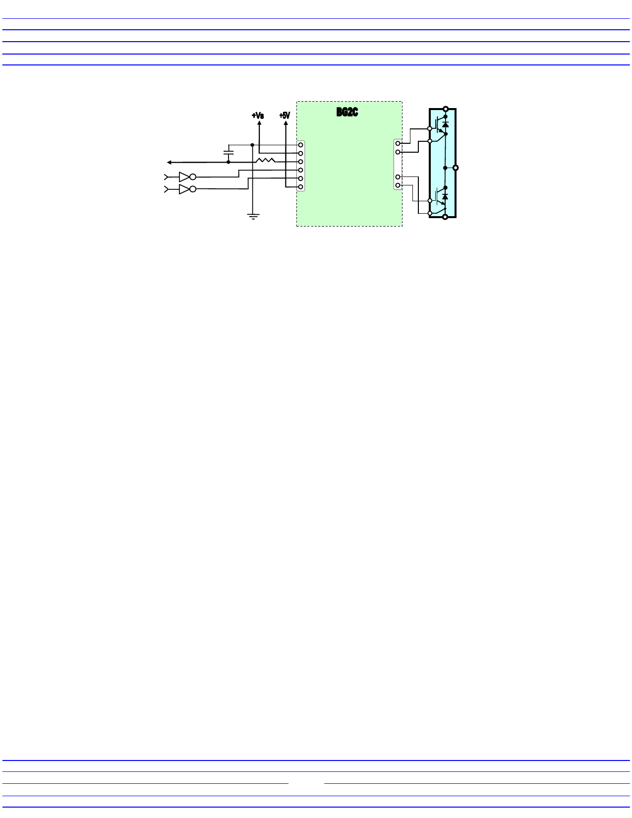
Figure 4: BG2C External Wiring Diagram
C1
To logic
level control
circuits
RC Filter to
remove noise on
fault signal
RC~10us
CMOS type
buffer must sink
15mA
CN1
GND
+VS
FO
IN1
IN2
+VL
CN2
G1
E1
E2
G2
C2E1
E2
IGBT Module
A complete schematic and component selection guide for the BG2C is shown in Figure 3. The board
will normally be operated with two input voltage sources. A 5V logic source (+VL) provides drive for the high
speed opto-couplers inside the hybrid gate drivers. A control power supply (+VS) provides power for the gate
driver and is connected to the primary side of the DC to DC converters at pins 8, 9 and 10, 11. The +VS source
is decoupled with a low impedance electrolytic capacitor C1. The capacitor is connected close to the input pins
of the DC to DC converters to provide a stable, well-filtered DC source. A 390µF capacitor was selected for C1
to provide the required ripple current and filtering assuming a maximum driven load and a significant distance to
the main filter capacitor of the +VS supply. These capacitors will be larger than necessary if the driven load is
smaller or the VS supply main filter capacitors are nearby. The DC to DC converters provide isolated gate drive
power which consists of +15.8V (VCC) at pin 3 and -8.2 (VEE) at pin 1 with respect to common at pin 2. The gate
drive power supplies are decoupled using the low impedance electrolytic capacitors C2, C3, C4, and C5. It is
very important that these capacitors have low enough impedance and sufficient ripple current capability to
provide the required high current gate drive pulses. The 390µF low impedance capacitors used on the BG2C
are sized to supply 5A gate pulses at a 60 KHz rate. If the application is operating at lower frequency or lower
peak current it may be possible to reduce the size of these capacitors.
The isolated VEE and VCC supplies provided by the DC to DC converters are connected to the hybrid
gate drivers at pins 6 and 8 to provide gate drive power. The hybrid gate driver amplifies the control input signal
and produces high current gate drive at pin 7. The gate drive current is adjusted by selecting the appropriate
series gate resistance (RG). RG will normally be adjusted to provide suitable drive for the module being used
considering dynamic performance, losses and switching noise. For more information on selecting RG see
Powerex IGBT module application notes. Protection against gate voltage surges is provided by Z1, Z2, Z3, and
Z4. These zener diodes also help to control short circuit currents by shunting miller current away from the gate.
Interface Circuit Requirements: A typical interface circuit for the BG2C is shown in Figure 4. A single control
power supply (+VS) is connected to pin 5 of CN1 with its common at pin 6. This supply provides all of the gate
drive power for both channels via the hybrid DC to DC converters. The current drawn from the +VS supply will
vary from less than 100mA to more than 500mA depending on the switching frequency and size of IGBT being
driven. Consult the hybrid gate driver application notes for details on determining the required supply current for
the gate driver. The gate driver supply current can then be converted into current drawn from the +VS supply
using the efficiency specification on the DC to DC converter data sheet.
A 5V logic supply is connected at pin 1 of CN1 and shares the same common at pin 6 of CN1 as the 15V
control supply. The 5V supply is directly connected to pin 2 of the hybrid gate driver which is internally
connected to the anode of the LED in the high speed opto coupler.
The control signal interface is designed for use with standard 5V CMOS logic. The control input signals at
pins 2 and 3 of connector CN1 are used to turn the IGBTs on and off. These signals are active low which means
that the gate driver output will be high (IGBT on) when they are pulled low. These control pins are connected
directly to pin 1 of the hybrid gate driver which is connected internally through a 180Ω limiting resistor to the
cathode of the LED in the high speed opto coupler (see figure 1). When the control signal is pulled low, current
flows from the 5V logic supply through the LED to turn the gate driver’s output on. The control pins must be
pulled low with a buffer that is capable of sinking at least 16mA in order to turn on the high speed opto coupler
inside the hybrid gate driver. A CMOS buffer that actively pulls its output high in the off state (74HC04 or similar)
3
Share Link: 