VN16118 查看數據表(PDF) - Vaishali Semiconductor
零件编号
产品描述 (功能)
生产厂家
VN16118 Datasheet PDF : 10 Pages
| |||
VN16118
Preliminary
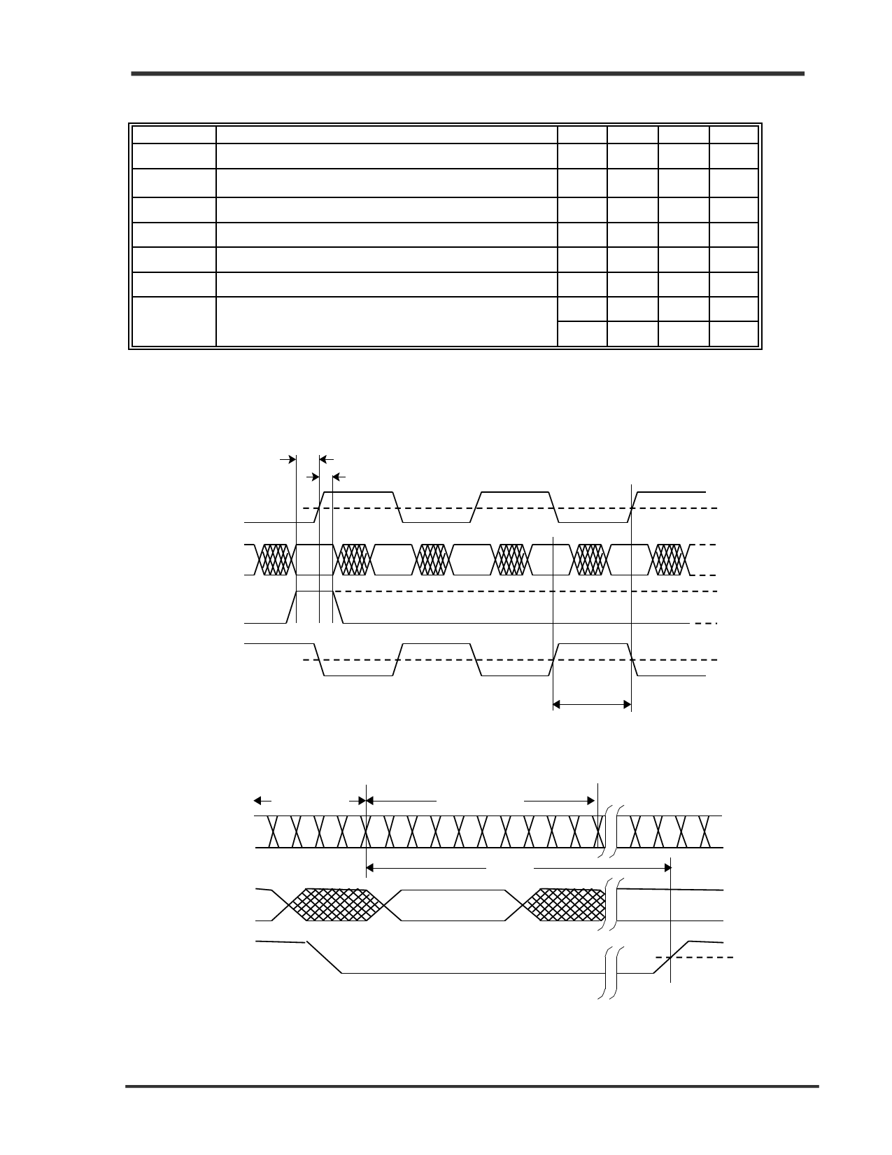
Table 8. Receiver Timing Characteristics
TA = 0°C to +70°C, Vcc = 3.15 V to 3.45 V
Symbol
b_sync[1]
Bit Sync Time
Parameter
Min. Typ. Max. Unit
2500 bits
f_lock
Frequency Lock at Powerup
500 µs
t SETUP
t HOLD
t DUTY
t A-B
T_rxlat[2]
Data Setup Before Rising Edge of RX_CLK
Data Hold After Rising Edge of RX_CLK
RX_CLK Duty Cycle
RX_CLK Skew
Receiver Latency
2.5
nsec
1.5
nsec
40
60
%
7.5
8.5 nsec
22.4
nsec
28.0
bits
Notes:
1. This is the recovery for input phase jumps.
2. The receiver latency as shown in Figure 6, is defined as the time between receiving the first serial bit of a
parallel data word (defined as the first edge of the first serial bit) and the clocking out of that parallel
word (defined by the rising edge of the receive byte clock, either RBC1 or RBC0).
tSETUP
RX_CLK<1>
tHOLD
RX<9:0>
COM_DET
K28.5
DATA
DATA
DATA
DATA
RX_CLK<0>
tA-B
Figure 5. Receiver Section Timing
1.4 V
2.0 V
0.8 V
2.0 V
0.8 V
1.4 V
DIN±
DATA BYTE C
DATA BYTE D
R5 R6 R7 R8 R9 R0 R1 R2 R3 R4 R5 R6 R7 R8 R9
RX<9:0>
t_rxlat
DATA BYTE A
R2 R3 R4 R5
DATA BYTE D
RX_CLK<1>/<0>
1.4 V
Figure 6. Receiver Latency
1999-12-15
Page 9
MDSN-0001-00
Vaishali Semiconductor l 747 Camden Avenue l Campbell l CA 95008 l Ph. 408.379.2900 l Fax 408.379.2937
Share Link: 