VSC7122 查看數據表(PDF) - Vitesse Semiconductor
零件编号
产品描述 (功能)
生产厂家
VSC7122
Vitesse Semiconductor

VSC7122 Datasheet PDF : 12 Pages
| |||
VITESSE
SEMICONDUCTOR CORPORATION
Quad Port Bypass Circuit for 1.0625 Gbit/sec
Fibre Channel Arbitrated Loop Disk Arrays
Advance Product Information
VSC7122
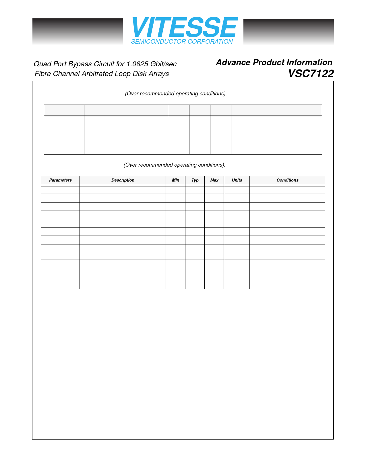
Table 2: AC Characteristics (Over recommended operating conditions).
Parameters
T1
T2
TSDR, TSDF
Description
Flow-Through Propagation Delay
Rising Edge to Rising Edge
Flow through Propagation Delay
Falling Edge to Falling Edge
Serial data rise and fall time
Min.
—
Max.
7.0
7.0
300
Units
ns
ns
ps.
Conditions
Delay with all circuits bypassed. 75
Ohm Load
Delay with all circuits bypassed. 75
Ohm load.
20% to 80%, tested on a sample basis
Table 3: DC Characteristics (Over recommended operating conditions).
Parameters
VIH(TTL)
VIL(TTL)
IIH(TTL)
IIL(TTL)
VDD
IDD
PD
∆VIN
∆VOUT50
∆VOUT75
Description
Min
Typ
Max
Units
Conditions
Input HIGH voltage (SEL - TTL)
Input LOW voltage (SEL - TTL)
2.0 — 5.5
0
— 0.8
V
IIH < 6.6 mA @ VIH = 5.5 V
V
—
Input HIGH current (SEL- TTL)
Input LOW current (SEL - TTL)
— 50 500
µA
VIN = 2.4 V
—
— -500
µA
VIN = 0.5 V
Supply voltage
3.10 — 3.50
V
VDD = 3.30V + 5%
Supply current
—
— 150
mA Outputs open, VDD = VDD max
Power Dissipation
0.35 0.5
W
Outputs open, VDD = VDD max
Receiver differential peak-to-peak
Input Sensitivity, IN+/- & L_SIn+/-
300
2600
mVp-p
AC Coupled.
Internally biased at VDD/2
Output differential peak-to-peak
voltage swing
1000 — 2200 mVp-p 50Ω to VDD – 2.0 V
Output differential peak-to-peak
voltage swing
1200
2200 mVp-p 75Ω to VDD – 2.0 V
Page 4
© VITESSE SEMICONDUCTOR CORPORATION
741 Calle Plano, Camarillo, CA 93012 • 805/388-3700 • FAX: 805/987-5896
G52155-0, Rev. 2.1
8/31/98
Share Link: