VSC7123QN 查看數據表(PDF) - Vitesse Semiconductor
零件编号
产品描述 (功能)
生产厂家
VSC7123QN Datasheet PDF : 18 Pages
| |||
VELOCITYTM
VITESSE
SEMICONDUCTOR CORPORATION
10-Bit Transceiver for Fibre
Channel and Gigabit Ethernet
Data Sheet
VSC7123
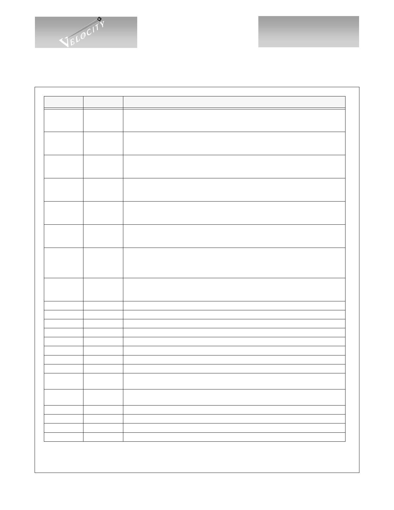
Pin #
62, 61
45,44,43,41
40,39,38,36
35,34
19
54, 52
31, 30
24
47
26
16, 17
49
48
55
56
27
18
15
5,10,20,23
28,50,57,59
1,14,21,25
51,58,64
29, 37, 42
32, 33, 46
60,63
53
Name
TX+, TX-
R0,R1,R2,R3
R4,R5,R6,R7
R8,R9
EWRAP
RX+, RX-
RCLK,
RCLKN
ENCDET
COMDET
SIGDET
CAP0, CAP1
TCK
TDI
TMS
TRSTN
TDO
VDDA
VSSA
Description
OUTPUTS - Differential PECL (AC-coupling recommended):
These pins output the serialized transmit data when EWRAP is LOW. When EWRAP is
HIGH, TX+ is HIGH and TX- is LOW.
OUTPUTS - TTL:
10-bit received character. Parallel data on this bus is clocked out on the rising edges of
RCLK and RCLKN. R0 is the first bit received on RX+/RX-.
INPUT - TTL:
LOW for normal operation. When HIGH, an internal loopback path from the transmitter to
the receiver is enabled. TX+ is held HIGH and TX- is held LOW.
INPUTS - Differential PECL (AC-coupling recommended):
The serial receive data inputs selected when EWRAP is LOW. Internally biased to VDD/2,
with 3.3KΩ resistors from each input pin to VDD and GND.
OUTPUT - Complementary TTL:
Recovered clocks derived from 1/20th of the RX+/- data stream. Each rising transition of
RCLK or RCLKN corresponds to a new word on R(0:9).
INPUT - TTL:
Enables COMDET and word resynchronization when HIGH. When LOW, keeps current
word alignment and disables COMDET.
OUTPUT - TTL:
This output goes HIGH for half of an RCLK period to indicate that R(0:9) contains a comma
character (‘0011111XXX’). COMDET will go HIGH only during a cycle when RCLKN is
rising. COMDET is enabled by ENCDET being HIGH.
OUTPUT - TTL
SIGnal DETect. This output goes HIGH when the RX input contains a valid Fibre Channel or
Gigabit Ethernet signal. A LOW indicates an invalid signal.
ANALOG: Differential capacitor for the CMU’s VCO, 0.1 µF nominal.
INPUT - TTL: JTAG clock input. Not normally connected.
INPUT - TTL: JTAG data input. Not normally connected.
INPUT - TTL: JTAG mode select input. Normally tied to VDDD
INPUT - TLL: JTAG reset input. Tie to VSSD for normal operation.
OUTPU - TTL: JTAG data output. Normally tri-stated.
Analog Power Supply
Analog Ground
VDDD
Digital Logic Power Supply
VSSD
VDDT
VSST
VDDP
N/C
Digital Logic Ground
TTL Output Power Supply
TTL Output Ground
PECL I/O Power Supply
No internal connection
Page 14
© VITESSE SEMICONDUCTOR CORPORATION • 741 Calle Plano • Camarillo, CA 93012
Tel: (800) VITESSE • FAX: (805) 987-5896 • Email: prodinfo@vitesse.com
Internet: www.vitesse.com
G52212-0, Rev 4.3
03/25/01
Share Link: 