VSC7124 查看數據表(PDF) - Vitesse Semiconductor
零件编号
产品描述 (功能)
生产厂家
VSC7124 Datasheet PDF : 8 Pages
| |||
VITESSE
SEMICONDUCTOR CORPORATION
Advance Product Information
VSC7124
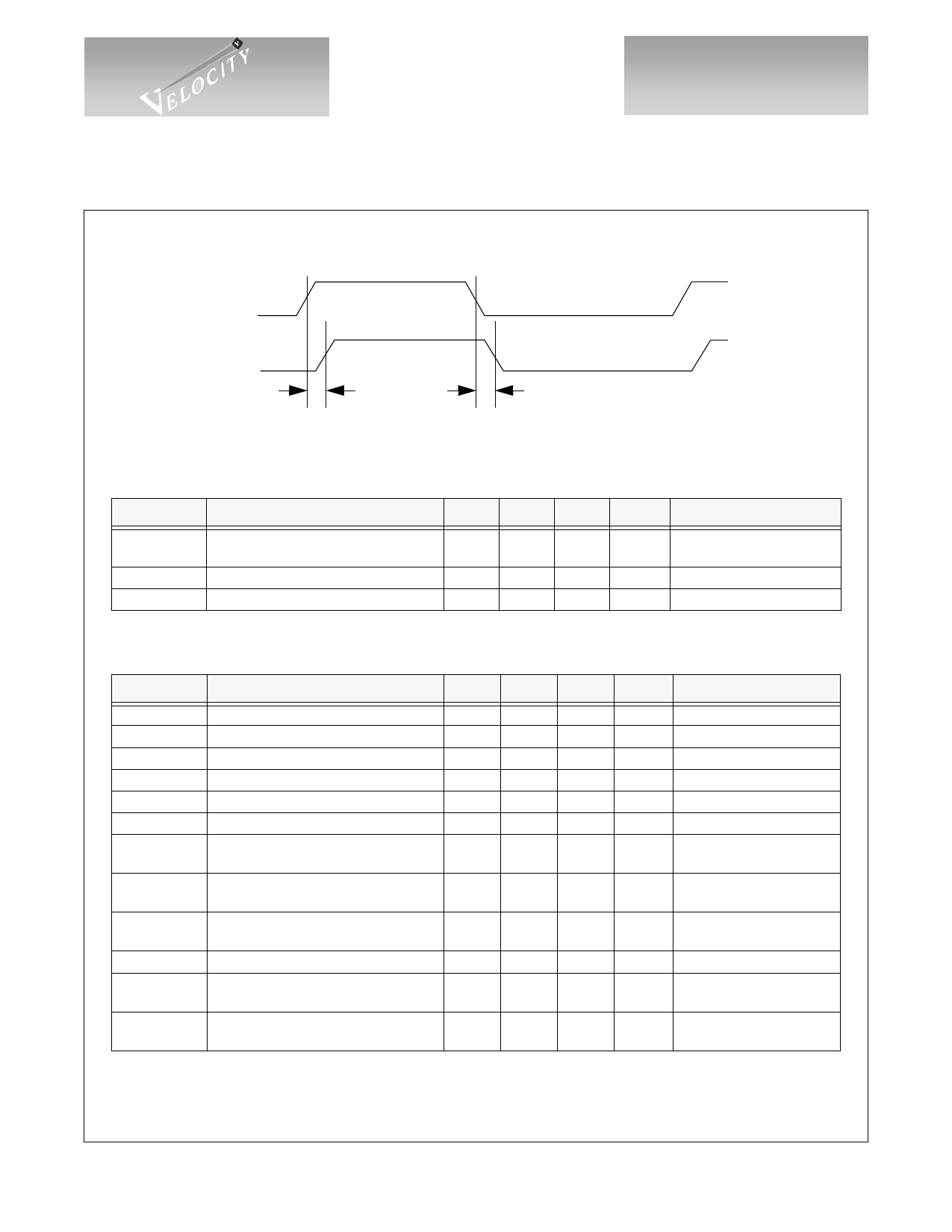
Figure 2: Timing Waveforms
Quad Port Bypass Circuit
Ix+/-
Ox+/-
T1
T1
AC Characteristics (Over Recommended Operating Conditions)
Parameters
Description
T1
TR, TF
Tj(PBC)
Propagation Delay
Serial Data Rise and Fall Time
Data Jitter Accummulation
Min Typ Max Units
Conditions
7.0
ns
Delay with all circuits
bypassed.
300
ps At ∆VIN minimum levels
120
ps Peak-to-Peak on Ox+/-
DC Characteristics (Over Recommended Operating Conditions)
Parameters
Description
Min Typ Max Units
Conditions
VOH
VOL
VIH
VIL
IIH
IIL
∆VOUT75(1)
∆VOUT50(1)
∆VIN(1)
VDD
PD
IDD
Output HIGH voltage (TTL)
Output LOW voltage (TTL)
Input HIGH voltage (TTL)
Input LOW voltage (TTL)
Input HIGH current (TTL)
Input LOW current (TTL)
TX output differential peak-to-peak
voltage swing
TX output differential peak-to-peak
voltage swing
Receiver differential peak-to-peak
Input Sensitivity RX
Supply voltage
Power dissipation
Power Supply Current
2.4
V
IOH = -1.0 mA
0.5
V
IOL = +1.0 mA
2.0
5.5
V
0
0.8
V
50
500
µA VIN =2.4V
-500
µA VIN =0.5V
1200
2200 mVp-p 75Ω to VDD – 2.0 V
1000
2200 mVp-p 50Ω to VDD – 2.0 V
400
2600 mVp-p Internally biased to VDD/2
3.14
3.47
V 3.3V±5%
250
555
mW
Outputs open,
VDD = VDD max ±2%
76
160
mA
Outputs open,
VDD = VDD max
NOTE: (1) Refer to Application Note AN-37 for details regarding differential voltage measurements.
G52293-0, Rev 2.3
05/07/01
© VITESSE SEMICONDUCTOR CORPORATION • 741 Calle Plano • Camarillo, CA 93012
Tel: (800) VITESSE • FAX: (805) 987-5896 • Email: prodinfo@vitesse.com
Internet: www.vitesse.com
Page 3
Share Link: 