VSC7126 查看數據表(PDF) - Vitesse Semiconductor
零件编号
产品描述 (功能)
生产厂家
VSC7126 Datasheet PDF : 16 Pages
| |||
1.0625 Gbits/sec Fibre
Channel Transceiver
VITESSE
SEMICONDUCTOR CORPORATION
Datasheet
VSC7126
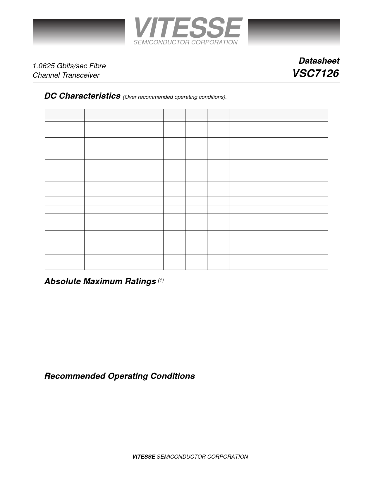
DC Characteristics (Over recommended operating conditions).
Parameters
Description
Min Typ Max Units
Conditions
VOH
Output HIGH voltage (TTL)
2.4
2.9
—
V IOH = -1.0 mA
VOL
Output LOW voltage (TTL)
—
—
0.5
V IOL = +1.0 mA
Serial Output voltage
∆VOUT75
differential peak-to-peak swing 1200
—
2200 mV 75Ω to VDD – 2.0 V
(TX+/TX-)
Serial Output voltage
∆VOUT50
differential peak-to-peak swing 1000
—
2200 mV 50Ω to VDD – 2.0 V
(TX+/TX-)
∆VIN
Serial Input voltage differential
peak-to-peak swing (RX+/RX-)
400
— 3200 mV
VIH
Input HIGH voltage (TTL)
VIL
Input LOW voltage (TTL)
IIH
Input HIGH current (TTL)
IIL
Input LOW current (TTL)
VDD
Supply voltage
PD
Power dissipation
IDD
Supply Current
2.0
—
5.5
V
0
—
0.8
V—
—
50
500
µA VIN = 2.4 V
—
—
-500
µA VIN = 0.5 V
3.14
— 3.47
V 3.3V±5%
—
850
1560
mW
Outputs open,
VDD = VDD max
—
245
450
mA
Outputs open,
VDD = VDD max
Absolute Maximum Ratings (1)
Power Supply Voltage, (VDD) ............................................................................................................-0.5V to +4V
DC Input Voltage (PECL inputs)............................................................................................ -0.5V to VDD +0.5V
DC Input Voltage (TTL inputs) ......................................................................................................... -0.5V to 5.5V
DC Output Voltage (TTL Outputs)........................................................................................ -0.5V to VDD + 0.5V
Output Current (TTL Outputs) ................................................................................................................. +/-50mA
Output Current (PECL Outputs)................................................................................................................+/-50mA
Case Temperature Under Bias .........................................................................................................-55o to +125oC
Storage Temperature..................................................................................................................... -65oC to +150oC
Maximum Input ESD (Human Body Model)............................................................................................... 1500V
Recommended Operating Conditions
Power Supply Voltage, (VDD) ................................................................................................................+3.3V+5%
Operating Temperature Range ................................................................0oC Ambient to 90oC Case Temperature
Notes:
(1) CAUTION: Stresses listed under “Absolute Maximum Ratings” may be applied to devices one at a time without causing
permanent damage. Functionality at or above the values listed is not implied. Exposure to these values for extended
periods may affect device reliability.
Page 8
© VITESSE SEMICONDUCTOR CORPORATION
741 Calle Plano, Camarillo, CA 93012 • 805/388-3700 • FAX: 805/987-5896
G52148-0, Rev. 4.3
3/4/99
Share Link: 