VSC7127R-QM 查看數據表(PDF) - Vitesse Semiconductor
零件编号
产品描述 (功能)
生产厂家
VSC7127R-QM Datasheet PDF : 12 Pages
| |||
VITESSE
SEMICONDUCTOR CORPORATION
Data Sheet
VSC7127/VSC7129
Family of Repeater/Retimer and Port
Bypass Circuits for Fibre Channel
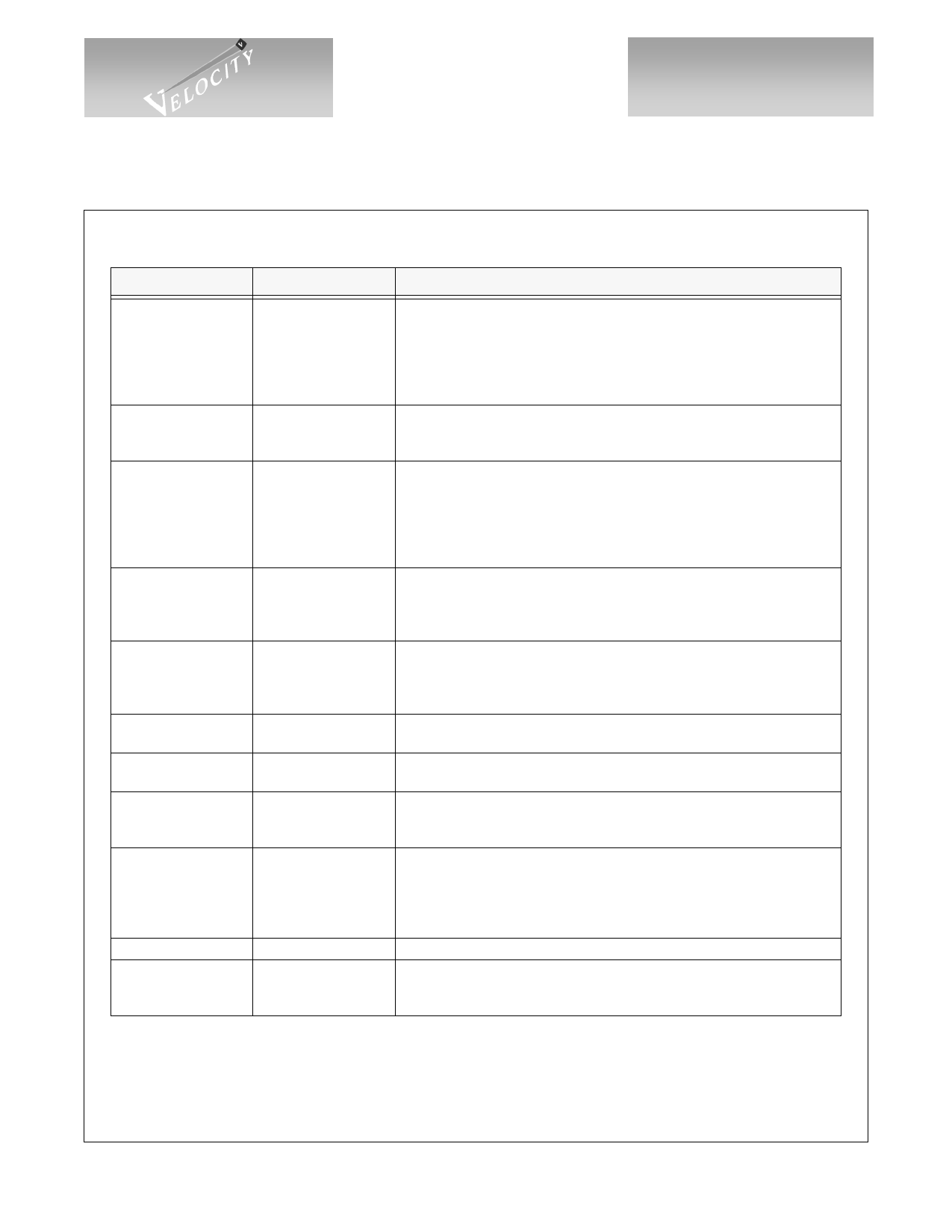
Table 4: Pin Identification
Pin #
Name
4, 3
41, 40
35, 34
28, 27
10, 9
15, 16,
17, 18
14, 22
7, 6
44, 43
38, 37
31, 30
24, 25
I1+, I1-
I2+, I2-
I3+, I3-
I4+, I4-
I0+, I 0-
SEL1, SEL2
SEL3, SEL4
SEL0, SEL5
O1+, O1-
O2+, O2-
O3+, O3-
O4+, O4-
O0+, O0-
13
REFCLK
12
20 (VSC7127)
19 (VSC7129
23 (VSC7127)
22 (VSC7129)
2
21 (VSC7127)
20 (VSC7129)
5
42
36
29
26
32
1, 8, 11, 33, 39
19 (VSC7127)
23 (VSC7129)
MODE
SIGDET
TRST
VDD
VDDP1
VDDP2
VDDP3
VDDP4
VDDP0
VDDA
VSS
Description
INPUT - Differential, internally biased to VDD/2.
I1+/I1- is the serial input to PBC1.
I2+/I2- is the serial input to PBC2.
I3+/I3- is the serial input to PBC3.
I4+/I4- is the serial input to PBC4.
I0+/I0- is the serial input to PBC0.
INPUT - TTL.
Port Bypass MUX SELect lines. A HIGH selects Ix. A LOW selects the
output of the previous internal device.
OUTPUT - Differential
O1+/O1- is the serial output from MUX1.
O2+/O2- is the serial output from PBC port 1.
O3+/O3- is the serial output from PBC port 2.
O4+/O4- is the serial output from PBC port 3.
O0+/O0- is the serial output from PBC port 4.
INPUT - TTL
106.25MHz REFerence CLocK for the internal Clock Multiplier PLL.
NOTE: A reference clock must be provided to the REFCLK pin in order for
the chip to power up in the right state
INPUT - TTL
(NOTE: Different for VSC7127T or VSC7127R)
In the VSC7127T, MODE configures the part as a Retimer if LOW or a
Repeater if HIGH. In the VSC7127R, MODE configures the parts as a
Repeater if LOW or a Retimer if HIGH. If unused, tie HIGH or LOW.
OUTPUT - TTL:
SIGnal DETect output
INPUT - TTL:
(Internal Pull-up Resistor)
Test mode input. Pull HIGH or leave open for normal operation.
Digital Logic Power Supply
Power Supply (3.3V) for O1+/-. If unused, connect to VSS.
Power Supply (3.3V) for O2+/-. If unused, connect to VSS.
Power Supply (3.3V) for O3+/-. If unused, connect to VSS.
Power Supply (3.3V) for O4+/-. If unused, connect to VSS.
Power Supply (3.3V) for O0+/-. If unused, connect to VSS
Analog Power Supply
Ground
G52298-0, Rev 4.3
05/01/01
© VITESSE SEMICONDUCTOR CORPORATION • 741 Calle Plano • Camarillo, CA 93012
Tel: (800) VITESSE • FAX: (805) 987-5896 • Email: prodinfo@vitesse.com
Internet: www.vitesse.com
Page 9
Share Link: 