VSC7146RH 查看數據表(PDF) - Vitesse Semiconductor
零件编号
产品描述 (功能)
生产厂家
VSC7146RH Datasheet PDF : 19 Pages
| |||
VITESSE
SEMICONDUCTOR CORPORATION
2.5Gb/s, 20-Bit Transceiver
Advance Product Information
VSC7146
Functional Description
Clock Synthesizer
The VSC7146 clock synthesizer multiplies the 125MHz reference frequency provided on the REF input by
20 to achieve a baud rate clock at 2.5GHz. The clock synthesizer contains a fully monolithic PLL which
requires no external components. An additional 125MHz clock, TBC, should be provided to clock in the data
bus. Since TBC is only used for the purpose of clocking data in, it is not required to have the same jitter
constraints as REF. REF clock and TBC should preserve certain phase margins and be of the same frequency.
Serializer
The VSC7146 accepts TTL input data as two parallel 10-bit characters on the T[0:19] bus which is latched
into the input latch on the rising edge of a 125MHz clock at TBC. This data will be serialized and transmitted on
the TX differential outputs at a baud rate of 20 times the frequency of the TBC input, with bit T0 transmitted
first. User data should be encoded for transmission using the 8B/10B block code described in the Fibre Channel
specification, or an equivalent, edge rich, DC-balanced code. If EWRAP is HIGH, the transmitter will be
disabled with TX+ HIGH and TX- LOW. If EWRAP is LOW, the transmitter outputs serialized data. The
phases of REF clock and TBC can be identical, but there is a phase relationship between the two input clocks
which must be maintained.
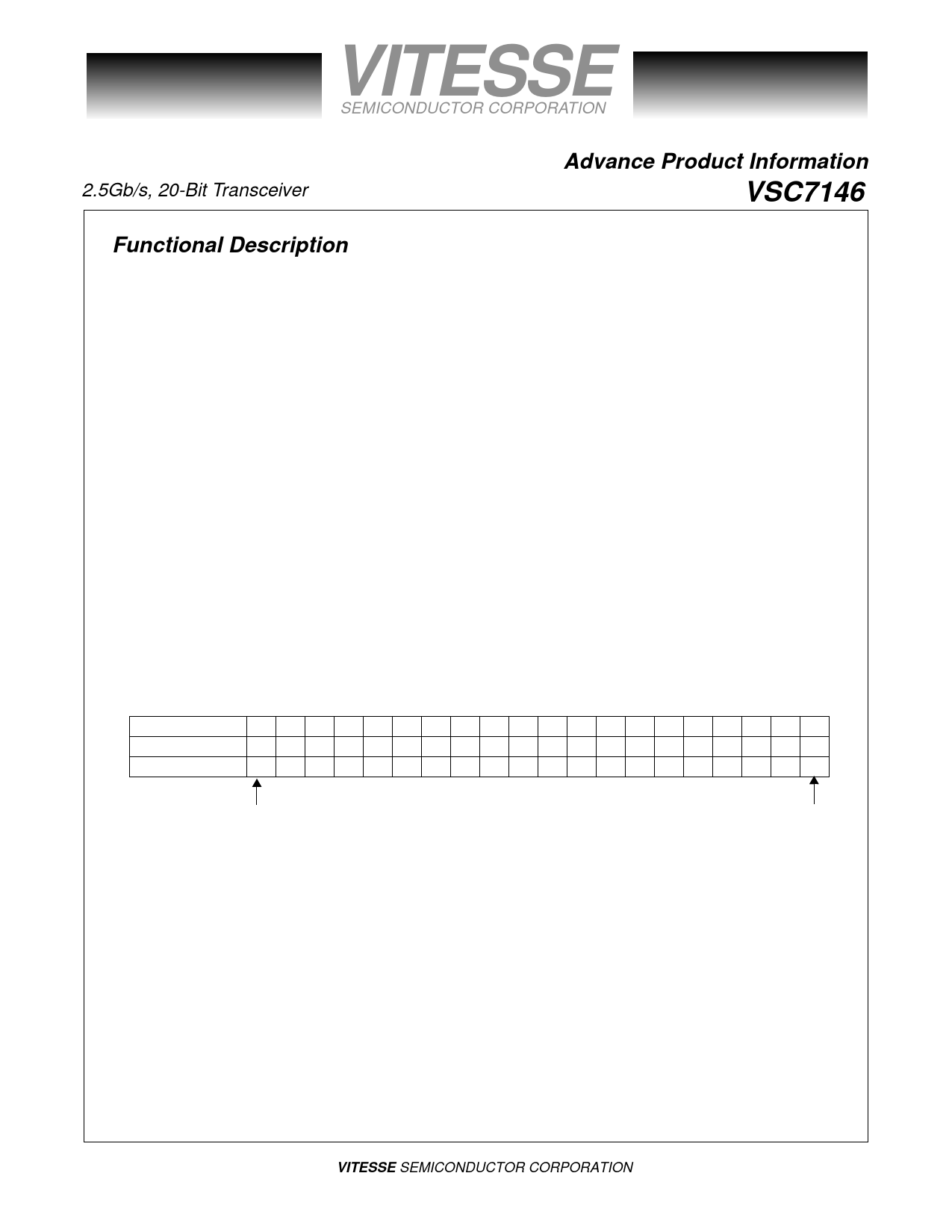
Transmission Character Interface
In Fibre Channel, an encoded byte is 10 bits and is referred to as a transmission character. The 20-bit
interface on the VSC7146 corresponds to two transmission characters. This mapping is shown in Figure 1.
Figure 1: Transmission Order and Mapping to Fibre Channel Character
Parallel Data Bits
19 18 17 16 15 14 13 12 11 10 09 08 07 06 05 04 03 02 01 00
8B/10B Bit Position
j hgf i edcba j hgf i edcba
Valid “Comma” Position
1111100
Last Data Bit Transmitted
First Data Bit Transmitted
Clock Recovery
The VSC7146 accepts differential high-speed serial inputs on the RX+/RX- pins, (when EWRAP is LOW),
extracts the clock and retimes the data. The serial bit stream should be encoded so as to provide DC balance and
limited run length by a Fibre Channel-compatible 8B/10B transmitter or equivalent. The VSC7146 clock
recovery circuitry is completely monolithic and requires no external components. For proper operation, the
baud rate of the data stream to be recovered should be within 200ppm of twenty times the REF frequency. This
allows oscillators on either end of the link to be 125MHz +/- 100ppm.
Page 2
© VITESSE SEMICONDUCTOR CORPORATION
741 Calle Plano, Camarillo, CA 93012 • 805/388-3700 • FAX: 805/987-5896
G52162-0 Rev. 2.7
8/28/00
Share Link: 