VSC8117QP 查看數據表(PDF) - Vitesse Semiconductor
零件编号
产品描述 (功能)
生产厂家
VSC8117QP
ATM/SONET/SDH 622/155 Mb/s Transceiver Mux/Demux with Integrated Clock Generation and Clock Recovery
Vitesse Semiconductor

VSC8117QP Datasheet PDF : 22 Pages
| |||
VITESSE
SEMICONDUCTOR CORPORATION
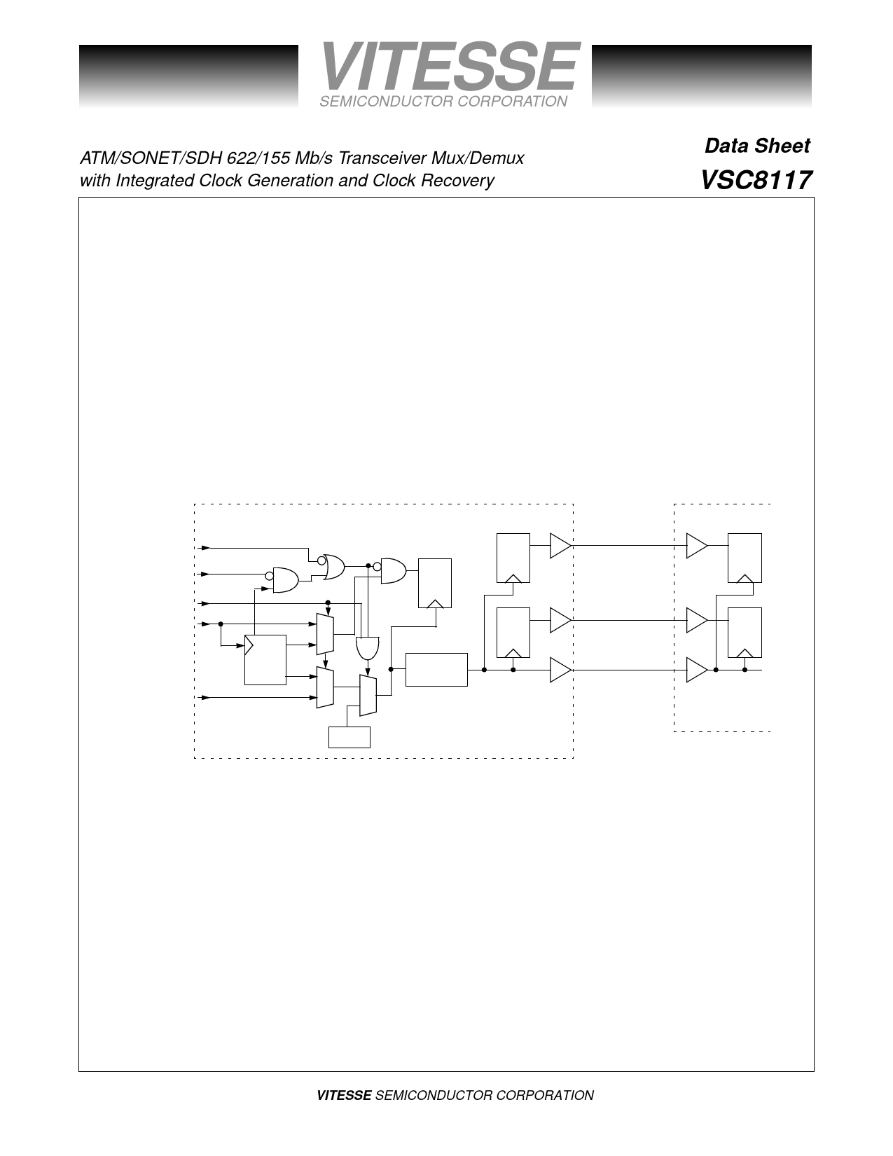
ATM/SONET/SDH 622/155 Mb/s Transceiver Mux/Demux
with Integrated Clock Generation and Clock Recovery
Data Sheet
VSC8117
Loss of Signal
The VSC8117 features Loss of Signal (LOS) detection. Loss of Signal is declared if the incoming serial
data stream has no transition continuously for more than 128 bits. During an LOS condition, the VSC8117
forces the receive data low which is an indication for any downstream equipment that an optical interface failure
has occurred. The receive section continues to be clocked by the CRU as it is now locked to the CRUREFCLK
unless DSBLCRU is active or CRUREFSEL is inactive in which case it will be clocked by the CMU. This LOS
condition will be removed when the part detects more than 16 transitions in a 128 bit time window. This LOS
detection feature can be disabled by applying a high level to the LOSDETEN_ input. The VSC8117 also has a
PECL input LOSPECL to force the part into a Loss of Signal state. Most optics have a PECL output usually
called “SD” or “FLAG” indicating a lack of or presence of optical power. Depending on the optics manufacturer
this signal is either active high or active low. The LOSPECL input on the VSC8117 is active low.
Figure 2: Data and Clock Receive Block Diagram
LOSPECL
LOSDETEN_
DSBLCRU
RXDATAIN+/-
RXCLKIN+/-
VSC8117
DQ
DQ
CRU
1
0
0
0
1
1
CMU
Divide-by-8
DQ
RXOUT[7:0]
PM5355
DQ
FP
RXLSCKOUT
DQ
Facility Loopback
The Facility Loopback function is controlled by the FACLOOP signal. When the FACLOOP signal is set
high, the Facility Loopback mode is activated and the high speed serial receive data (RXDATAIN) is presented
to the high speed transmit output (TXDATAOUT). See Figure 3. In Facility Loopback mode the high speed
receive data (RXDATAIN) is also converted to parallel data and presented to the low speed receive data output
pins (RXOUT[7:0]). The receive clock (RXCLKIN) or the recovered clock is also divided down and presented
to the low speed clock output (RXLSCKOUT).
Page 4
© VITESSE SEMICONDUCTOR CORPORATION
741 Calle Plano, Camarillo, CA 93012 • 805/388-3700 • FAX: 805/987-5896
G52221-0, Rev 4.1
1/8/00
Share Link: