VSC8021FI 查看數據表(PDF) - Vitesse Semiconductor
零件编号
产品描述 (功能)
生产厂家
VSC8021FI Datasheet PDF : 17 Pages
| |||
VITESSE
SEMICONDUCTOR CORPORATION
2.5Gb/s SONET-Compatible
8-Bit MUX/DEMUX Chipset
Data Sheet
VSC8021/VSC8022
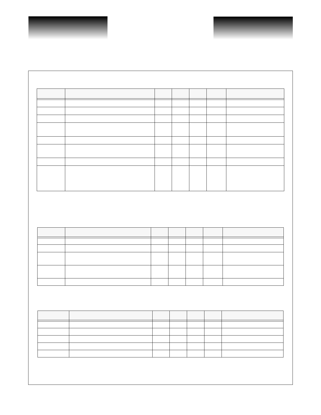
Table 2: VSC8022 Demultiplexer AC Characteristics
Parameter
Description
Min Typ Max Units
tC
tD
tBD
tDFP
tPFP
tOOFN
tOOFNPW
Phase
Margin
Clock period(1)
400
BYTE clock period (tD = tC x 8) (framed)
BYTE clock output to valid data
3.2
0.5 1.0
FP rising edge from parallel data output
change from A1 to A2 (tDFP = tD)
3.2
FP pulse width (tPFP = tD)
3.2
OOFN falling edge before A1 chan
ges to A2 (tOOFN = tD x 4)
12.8
OOFN pulse width (tOOFNPW = tD)
3.2
Serial data phase timing margin with respect
to high-speed clock:
Phase Margin = 1 – t--S---U---t--C+-----t--H-- 360°
135 180
ps
ns
2.0
ns
ns
ns
ns
ns
degrees
NOTE: (1) If t C changes, all the remaining parameters change as indicated by the equations.
Conditions
DC Characteristics
Table 3: Low Speed ECL Inputs and Outputs
(Over recommended operating range with internal VREF, VCC = GND, output load = 50Ω to -2.0V)
Parameter
Description
Min Typ Max Units
Conditions
VOH
Output HIGH voltage
VOL
Output LOW voltage
VIH
Input HIGH voltage
-1020
VTT
-1150
-700
-1620
-600
mV VIN = VIH (max) or VIL (min)
mV VIN = VIH (max) or VIL (min)
mV
Guaranteed HIGH signal for
all inputs
VIL
Input LOW voltage
VTT
-1500
mV
Guaranteed LOW signal for
all inputs
∆VOUT
Output voltage swing
0.8 1.0 1.4
Note: Differential ECL output pins must be terminated identically.
V Output load 50Ω to VTT
Table 4: High-Speed Inputs and Outputs
(Over recommended operating conditions, VCC = GND, Output load = 50Ω to -2.0V)
Parameter
Description
Min Typ Max Units
Conditions
∆VIN
Input voltage swing
0.8 1.0 1.2
V AC-coupled
VOH
Output HIGH voltage
-0.9
V Output load, 50Ω to -2.0V
VOL
Output LOW voltage
-1.8
V Output load, 50Ω to -2.0V
∆VOUT(DATA) Output voltage swing for data
0.6 0.8 1.2
V Output load, 50Ω to -2.0V
∆VOUT(clk) Output voltage swing for clock
0.6 0.7 1.2
V Output load, 50Ω to -2.0V
NOTES: (1) A reference generator is built in to each high-speed input, and these inputs are designed to be AC-coupled.
(2) If a high-speed input is used single-ended, a 150pF capacitor must be connected between the unused high-speed or comple-
ment input and the power supply (VTT).
(3) Differential high-speed outputs must be terminated identically.
Page 6
© VITESSE SEMICONDUCTOR CORPORATION • 741 Calle Plano • Camarillo, CA 93012
Tel: (800) VITESSE • FAX: (805) 987-5896 • Email: prodinfo@vitesse.com
Internet: www.vitesse.com
G52028-0, Rev 4.1
05/25/01
Share Link: 