VSC8022FC 查看數據表(PDF) - Vitesse Semiconductor
零件编号
产品描述 (功能)
生产厂家
VSC8022FC Datasheet PDF : 17 Pages
| |||
VITESSE
SEMICONDUCTOR CORPORATION
2.5Gb/s SONET-Compatible
8-Bit MUX/DEMUX Chipset
Data Sheet
VSC8021/VSC8022
VSC8022 SONET Frame Recovery and Detection
The SONET framing sequence is a string of A1 bytes followed by a string of A2 bytes. (A1 = 11110110 and A2
= 00101000). The first serial bit starts at the left of the byte. Table 6 shows the number of A1 and A2 bytes in each
SONET frame for different line rates. The VSC8022 contains a frame recovery circuit and a frame detection circuit.
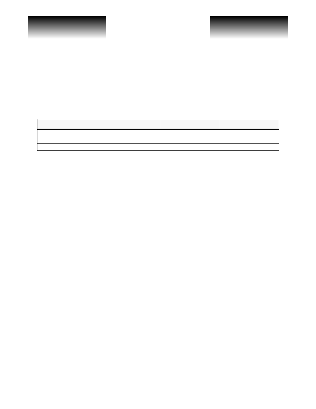
Table 6: A1/A2 Byte Count
STS Level
STS-3
STS-12
STS-48
Line Rate (Mb/s)
155.520
622.080
2488.32
# of A1 Bytes
3
12
48
# of A2 Bytes
3
12
48
Frame Recovery Circuit
The frame recovery circuit is designed to scan the serial data stream, looking for the A1 byte. When it finds
the A1 pattern, it adjusts internal timing so that the serial data is properly demultiplexed onto the eight parallel
outputs. Subsequently, the MSB of the A1 byte will appear in the D1 position and LSB of the A1 byte will
appear in the D8 position. This word boundary alignment causes the BYCKO, BYCKON output to be resyn-
chronized. While the frame aligner is hunting for the frame, BYCKO and parallel data are invalid. Frame recov-
ery circuits are disabled by frame detection (resulting in FP) or by a falling edge on the OOFN input while FDIS
is high.
Frame Detection Circuit
The frame detection circuit monitors the demultiplexed data, and senses the boundary between A1 and A2
bytes. This pulse on the FP output will reset the frame recovery circuit, so that no further resynchronization will
occur until permission is given through OOFN.
Circuit Operation
The frame recovery circuits are initialized and enabled on the falling edge of the OOFN ECL input with
FDIS held low. The OOFN must be at least one byte clock period wide. It must occur at least four byte clock
periods before the A1/A2 boundary. The circuit requires at least three A1 bytes followed by 3 A2 bytes for suc-
cessful alignment. The first A1 byte is used by the frame recovery circuit to obtain initial word boundary align-
ment, while the following two A1 and three A2 bytes are used to reset the frame recovery circuit and maintain
alignment for the subsequent bit stream. Frame recognition will occur for each word boundary aligned
A1A1A2A2A2 sequence in the data stream. Frame recognition is signaled by a one byte clock period high pulse
on the FP ECL output pin. This FP pulse will appear one byte period after the first A2 byte appears on the paral-
lel data output pins.
Page 8
© VITESSE SEMICONDUCTOR CORPORATION • 741 Calle Plano • Camarillo, CA 93012
Tel: (800) VITESSE • FAX: (805) 987-5896 • Email: prodinfo@vitesse.com
Internet: www.vitesse.com
G52028-0, Rev 4.1
05/25/01
Share Link: 