VSC837UG 查看數據表(PDF) - Vitesse Semiconductor
零件编号
产品描述 (功能)
生产厂家
VSC837UG Datasheet PDF : 26 Pages
| |||
VITESSE
SEMICONDUCTOR CORPORATION
3.2Gb/s
68x68 Crosspoint Switch
Preliminary Data Sheet
VSC837
DC Characteristics
All characteristics are over the specified operating conditions.
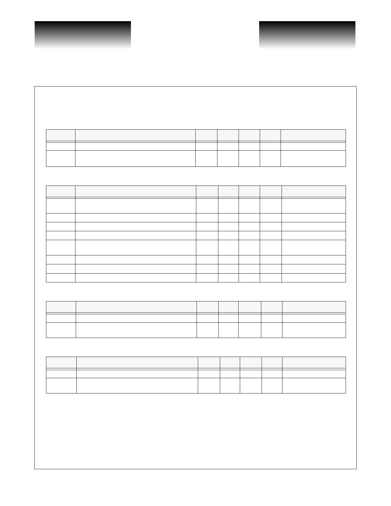
Table 3: Power Supply Requirements
Symbol
ICC
PT
Parameter
VCC supply current
Total chip power (with ITERM = 0 and back-
terminations ON, high drive)
Min Typ Max Units
5600 6095 mA
13
16
W
Conditions
Table 4: Control Port Input Levels (TTL/CMOS)
Symbol
Parameter
VIH
VIL
IIH
IIL
VOH
VOL
VOHPU
VOLPU
Input HIGH voltage
Input LOW voltage
Input HIGH current
Input LOW current
Output HIGH voltage
Output LOW voltage
VOH with external pull-up
VOL with external pull-up
Min Typ Max Units
Conditions
1.7
0
VCC-
0.2
0
2.4
VCC+
1.0
0.8
TBD
TBD
VCC
0.2
0.4
V
V
µA
µA
V DC load < 500µA
V DC load < 2mA
V 250Ω to 3.3V(5%)
V 250Ω to 3.3V(5%)
Table 5: Signal Input Levels (high-speed signal path)
Symbol
VIN
VICM
Parameter
Input voltage amplitude
Input common-mode voltage
Min Typ Max Units
Conditions
150
VCC -
0.7
1100
VCC -
0.2
mV See Note 1
V See Note 2
Table 6: Signal Output Levels (high-speed signal path) TERM_CTRL=ON, DRIVE_CTRL=HI
Symbol
VOUT
VOCM
Parameter
Output differential voltage
Output common-mode voltage
Min Typ Max Units
Conditions
400
VCC-
0.3
600
VCC-
0.2
mV See Note 1, 3
V See Note 2, 3
NOTES: (1) Mean peak-to-peak amplitude measurement of either true or complement of the differential signal. (2) VCC = VCCP = 2.5V, VEE = 0V.
(3) Terminated in 50Ω to VCC. This termination is used for testing the part, but other terminations are allowed—see Table 9.
Page 8
© VITESSE SEMICONDUCTOR CORPORATION • 741 Calle Plano • Camarillo, CA 93012
Tel: (800) VITESSE • FAX: (805) 987-5896 • Email: prodinfo@vitesse.com
Internet: www.vitesse.com
G52309-0, Rev 3.0
02/16/01
Share Link: 