VSC880 查看數據表(PDF) - Vitesse Semiconductor
零件编号
产品描述 (功能)
生产厂家
VSC880 Datasheet PDF : 28 Pages
| |||
VITESSE
SEMICONDUCTOR CORPORATION
High Performance 16x16
Serial Crosspoint Switch
Data Sheet
VSC880
General Description
The VSC880 is a 16x16 serial crosspoint switch with serial data rates at 2.125Gb/s. The VSC880 has been
designed to operate with the VSC870 backplane transceiver to establish a synchronous high performance switching
system with an aggregate bandwidth of 32Gb/s. The switch chip transmits the master word clock (62.5Mb/s), and
master cell clock (if used) to all port cards through the serial data channels. The transceivers automatically perform
bit alignment, word alignment and cell alignment to the switch chip. The transceiver and switch chip have been
optimized for both self-routing and cell-based systems and include special commands for connection requests (self-
routing) and cell synchronous operation (cell based). In addition, a parallel CPU interface can be used to control
internal modes and read status information from the switch. A 20-bit interface can also be used to program the switch
matrix in 4 clock cycles. The switch chip runs off of a 3.3V/2.5V or 3.3V/2.0V power supplies. The serial I/O buffers
contain on-chip termination resistors (see Application Note 34).
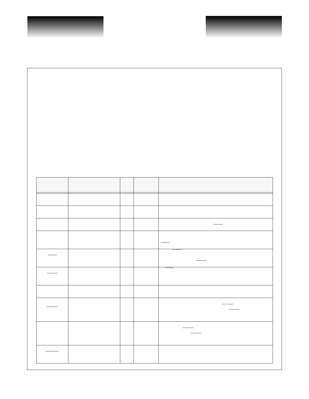
Pin Descriptions
Pin
Name
I/O
Freq
Type
Description
TXS[15:0]+/
TXS[15:0]-
Transmit Serial Outputs
O
2.125Gb/s
LVDS
16 high speed serial differential transmit channels
RXS[15:0]+/
RXS[15:0]-
Receive Serial Inputs
I
2.125Gb/s
LVDS
16 high speed serial differential receive channels
DATA[15:0] Configuration Data Input I
62.5Mb/s Parallel input signals used to program the switch matrix in 4
TTL clock cycles when the signal CEN is LOW.
FI[3:0]
Force IDLE Input
I
62.5Mb/s
TTL
Parallel input signals used to program force IDLE words at
the switch matrix output in 4 clock cycles when the signal
CEN is LOW.
CEN
Configure Enable
I
62.5Mb/s
TTL
When CEN is held LOW, the inputs DATA[15:0] and FI[3:0]
can be used to program the switch matrix in 4 word clock
cycles timed to the WEN signal.
WEN
Write Enable
I
62.5Mb/s
TTL
If CEN is LOW, this signal provides a synchronization pulse
for loading switch configuration data into DATA[15:0] and
FI[3:0].
ADDR[5:0]
Data Address
I
62.5Mb/s The address to read and write data through parallel interface
TTL CDATA[7:0].
CSEL
Chip Select
This signal allows several switch chips to share an 8 bit data
I
62.5Mb/s bus connected to CDATA[7:0]. If CSEL is LOW, data will
TTL be read or written to CDATA[7:0]. If CSEL is HIGH, the
outputs will be high impedance and the inputs disabled.
CDATA[7:0]
Status Data Output
Bidirectional CPU interface for the status and control
B
62.5Mb/s registers. If CSEL is LOW, the data will be read or written
TTL into this port. If CSEL is HIGH, the outputs will be high
impedance and the inputs will be disabled.
CWEN
Control Write Enable
I
62.5Mb/s
TTL
This signal is set HIGH to read the internal status registers
through the parallel interface CDATA[7:0]. It is set LOW to
write into this interface.
Page 2
© VITESSE SEMICONDUCTOR CORPORATION • 741 Calle Plano • Camarillo, CA 93012
Tel: (800) VITESSE • FAX: (805) 987-5896 • Email: prodinfo@vitesse.com
Internet: www.vitesse.com
G52191-0, Rev 4.2
01/05/01
Share Link: 