VSC880 查看數據表(PDF) - Vitesse Semiconductor
零件编号
产品描述 (功能)
生产厂家
VSC880 Datasheet PDF : 28 Pages
| |||
VITESSE
SEMICONDUCTOR CORPORATION
High Performance 16x16
Serial Crosspoint Switch
Data Sheet
VSC880
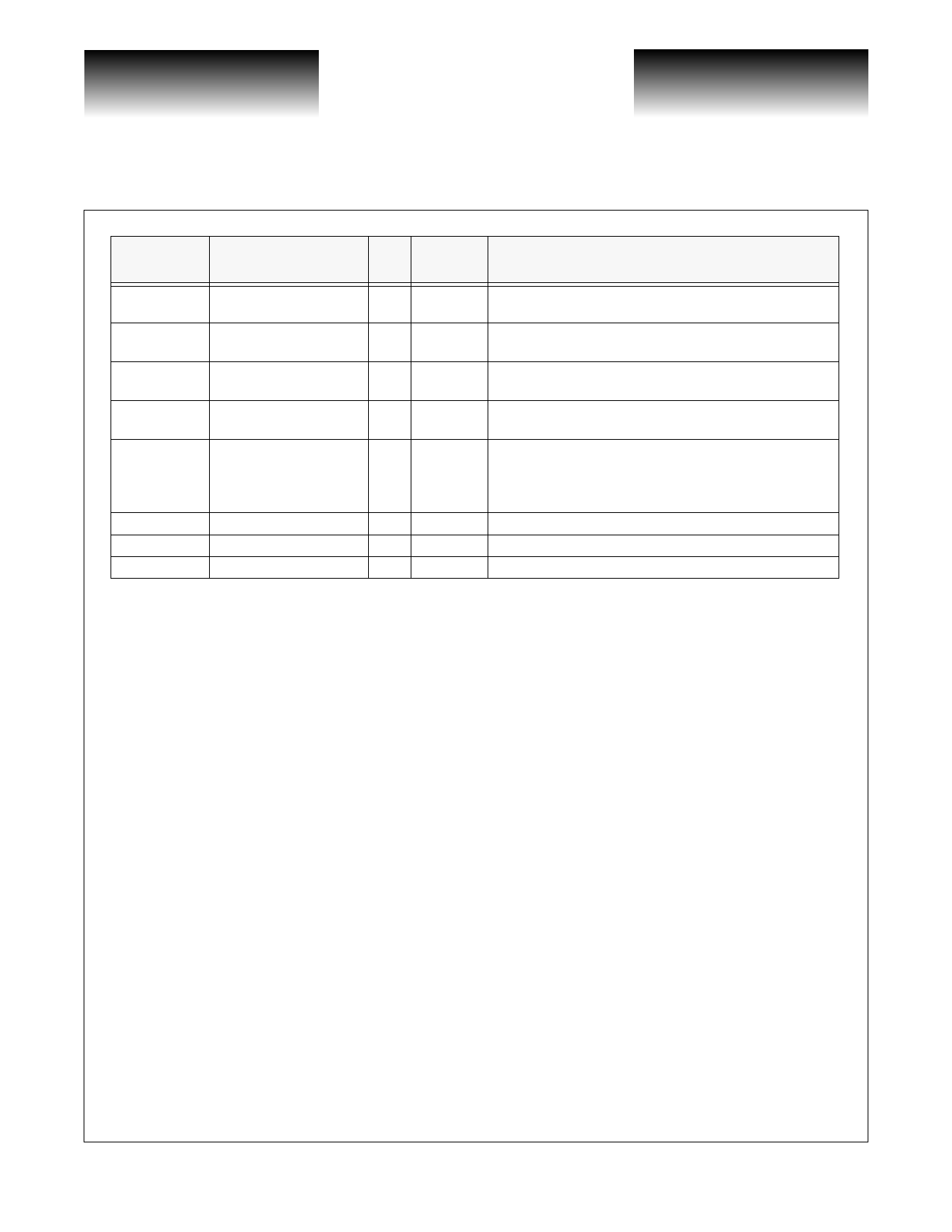
Pin
Name
I/O
Freq
Type
Description
LOCKDET
CMU Lock Detect
O
<1MHz
TTL
This signal is LOW while the CMU is acquiring lock.
VSCTE
NOR Chain Test Enable I
<1MHz Used for ATE testing of the parametric NOR chain in the I/O
TTL frame. Set to logic LOW during normal operation.
VSCIPNC
NOR Chain Input
I
<1MHz Used for ATE testing of the parametric NOR chain in the I/O
TTL frame. Set to logic LOW during normal operation.
VSCOPNC
NOR Chain Output
O
<1MHz Used for ATE testing of the parametric NOR chain in the I/O
VECL frame. Leave output open during normal operation.
VDD1, VDD2,
VDD3, VDD4
Serial Port Power
Supplies
VDD1 = Serial Port 0-3 power supply
P
3.3V
VDD2 = Serial Port 4-7 power supply
VDD3 = Serial Port 8-11 power supply
VDD4 = Serial Port 12-15 power supply
VDDA
CMU Power Supply
P
3.3V Clean power supply for CMU
VSSA
CMU Ground
P
0V Clean ground for CMU
VMM
Core Power Supply
P 2 ~ 2.5V Core power supply
Functional Description
The VSC880 switch can be used in conjunction with the VSC870 transceivers to support two modes of
operation: Packet Mode and Cell Mode. In Packet mode, the chip set provides a switching system to support variable
length, self-routing data packets. In Cell Mode, the chip set provides a cell synchronous switching system with a user
defined scheduler. In this mode, it can support only fixed length data packets (cells). Routing decisions are carried
out in the scheduler and crosspoint configuration is synchronized to a cell clock. The scheduler configures the switch
matrix using the parallel interface. To conserve power, each serial port quadrant can be powered down if not used.
The following section gives a detailed functional description of the operation of the switch chip. Most of the
discussion includes some of the transceiver operation (see the VSC870 data sheet). The two major operation modes
are described separately in the Packet Mode and the Cell Mode sections.
1.0 Common Features
1.1 Synchronization
1.1.1 Link Characteristic
The serial link is used to connect the switch chip to transceivers. These links operate at 2.125 Gb/s and are
initialized simultaneously at power up, or separately when a link error occurs. A link is first bit synchronized, then
word synchronized and, if CMODE is HIGH, cell synchronized. In Packet or Cell mode, the switch acts as the
master, generating the bit clock along with the word and cell boundary information. The transceivers act as slaves,
recovering the bit clock, word clock and cell clock. The transceiver also contains redundant serial inputs and outputs
which can be used with a redundant switch chip.
Page 4
© VITESSE SEMICONDUCTOR CORPORATION • 741 Calle Plano • Camarillo, CA 93012
Tel: (800) VITESSE • FAX: (805) 987-5896 • Email: prodinfo@vitesse.com
Internet: www.vitesse.com
G52191-0, Rev 4.2
01/05/01
Share Link: 