VSC880 查看數據表(PDF) - Vitesse Semiconductor
零件编号
产品描述 (功能)
生产厂家
VSC880 Datasheet PDF : 28 Pages
| |||
Data Sheet
VSC880
VITESSE
SEMICONDUCTOR CORPORATION
High Performance 16x16
Serial Crosspoint Switch
33 32
00
31 30 29
1BB
10
28 27 26 25 24
CCCCC
04 03 02 01 00
-- Command --
23 22 21 20
DDDD
15 14 13 12
19 18 17 16 15 14 13 12
DDDD
11 10 09 08
DDDD
07 06 05 04
-- Data --
11 10 09 08
DDDD
03 02 01 00
07 06 05 04
1010
Where:
B[1:0]00=Undefined (during normal operation) or alignment word
01=Flow control channel,
10=Flow control channel,
11=Acknowledge (from switch chip only) or link initialization reset or cell clock in cell mode
C[4:0]Command type
00XXX=Link Control (00000=ALIGN word, 00111=IDLE word)
01XX0=Command word for transceiver (01000=set DLYEN/CCKIN value)
10XX0=Command word for switch
11XX0=Command word for receiving port card (TBD)
D[15:0]Optional data payload
Default=1010101010101010
IDLE Word from switch=Current switch outputs this port is connected to
D[15] is for port 0, D[0] is for port 15
If C[4:0]=01000, D[3:0]=DLYEN/CCKIN value
03 02 01 00
1010
1.2.3 IDLE Words
IDLE words are the default word used on the serial channel when none of the other word types are present. In
most cases, these words are automatically generated by the transceiver or switch chip. In Packet Mode, IDLE words
are inserted between packets and the IDLE word from the switch always returns the current output connections for
the port that is receiving the IDLEs. These connection bits will be in the same location as in the CRQ word. In cell
mode, IDLEs will be transmitted from the switch chip if the force IDLE (FI) bit is set in the control registers. IDLE
words are also used to detect link error conditions. If the switch chip detects an IDLE word, it uses a bit mask to ver-
ify the proper bit pattern within the word.
1.3 Loopback
The VSC880 supports a loopback function at the serial interfaces which is used in built-in self-test mode. If the
BSTLPBK signal is set HIGH and TESTEN is set LOW, the serial transmit data is looped back to the serial receive
side for all 16 channels. If the BSTLPBK signal is set HIGH and TESTEN is set HIGH, the serial transmit data is
looped back to the serial receive side for channels 0-7 only. If the FACLPBK signal is set HIGH, the serial receive
signal is looped back to the serial output for all 16 channels. Each channel can also be programmed to be looped back
separately from serial input to serial output by using the control registers described below. The VSC880 does not
support simultaneous BIST and facilty loopback functions (either FACLPBK pin or LPBK[15:0] register).
1.4 Internal Register Definitions
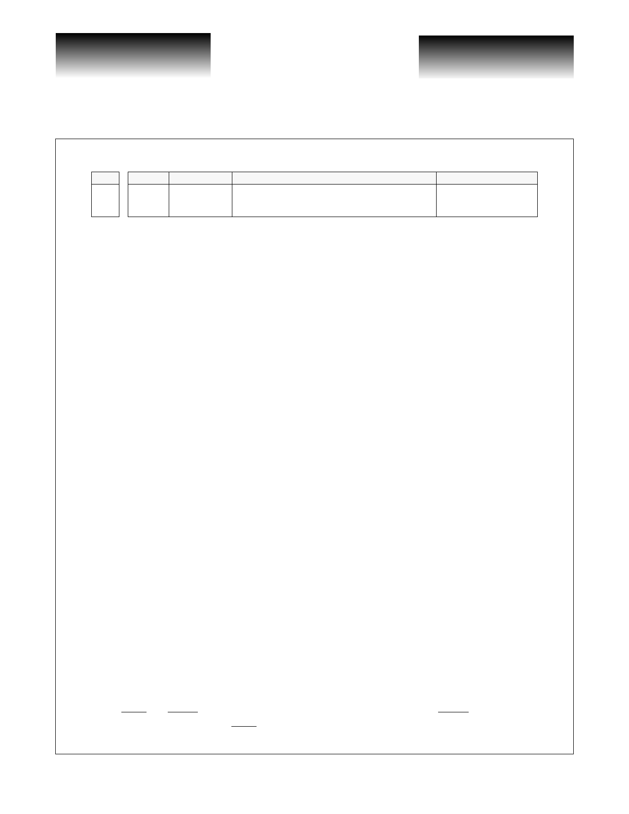
The internal status and control registers are defined in the following table. The address signal ADDR[5:0] is used
along with CSEL and CWEN to read or write data through the CDATA[7:0] interface. CWEN is set LOW to write
and HIGH to read from this port. If CSEL is HIGH, the outputs become high impedance and the inputs become
G52191-0, Rev 4.2
01/05/01
© VITESSE SEMICONDUCTOR CORPORATION • 741 Calle Plano • Camarillo, CA 93012
Tel: (800) VITESSE • FAX: (805) 987-5896 • Email: prodinfo@vitesse.com
Internet: www.vitesse.com
Page 7
Share Link: 