VSC880 查看數據表(PDF) - Vitesse Semiconductor
零件编号
产品描述 (功能)
生产厂家
VSC880 Datasheet PDF : 28 Pages
| |||
VITESSE
SEMICONDUCTOR CORPORATION
High Performance 16x16
Serial Crosspoint Switch
Data Sheet
VSC880
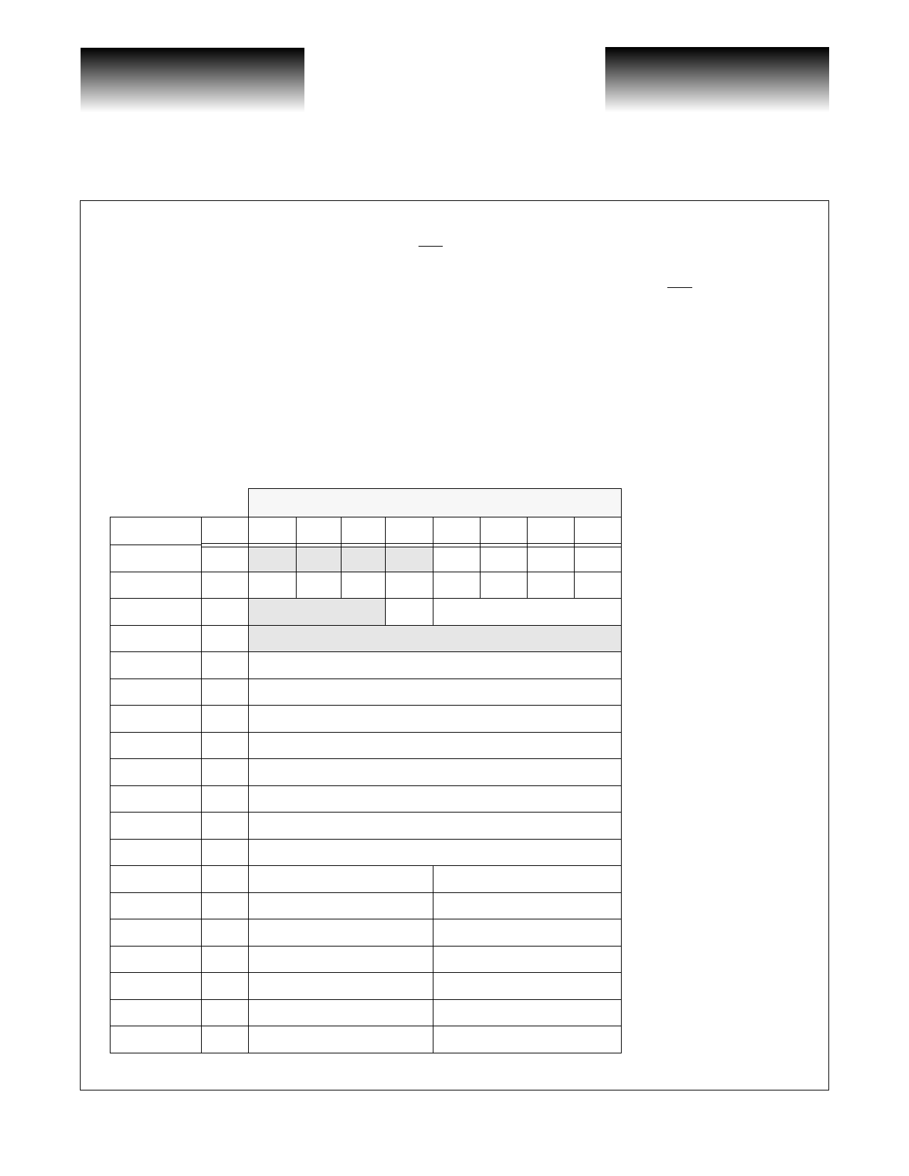
disabled. All data transfer timing is asynchronous to REFCLK. The Interrupt Control Register is written by the user
to mask certain operations. If ICE is set HIGH, the INT output pin will go LOW if any error bit is set in the CERR
register. If RCE is set HIGH, the link will automatically start link initialization if any error bit is set in the CERR
register. The corresponding pins can be used for the DERR, TERR and LERR registers. If the INT signal goes LOW,
the Interrupt Status Register can be read to determine which of the four registers received an error.
The CDEL[3:0] bits are used to program a value for the cell clock delay (see section 3.0). The switch matrix
status information can be read from the CN and FI registers. A serial link can be forced to reinitialize by writing a
HIGH into the RSY register. A serial output can be logically disabled by writing a HIGH into the OE register. A serial
input can be forced to loop back directly to a serial output by writing a HIGH into the LPBK register. All registers are
cleared upon RESET. Also, the LERR, TERR, DERR and CERR registers are cleared on reading.
Figure 1: Status and Control Register Definition
CDATA[7:0] Bit Position
ADDR[5:0] R/W 7
6
5
4
3
2
1
X00000 R
CE DE TE
X 0 0 0 0 1 R/W RCE RDE RTE RLE ICE IDE ITE
X 0 0 0 1 0 R/W
BIST
CDEL[3:0]
X 00011
X00100 R
CERR[7:0]
X00101 R
CERR[15:8]
X00110 R
DERR[7:0]
X00111 R
DERR[15:8]
X01000 R
TERR[7:0]
X01001 R
TERR[15:8]
X01010 R
LERR[7:0]
X01011 R
LERR[15:8]
0 0 1 1 0 0 R/W
C0[3:0]
C8[3:0]
0 0 1 1 0 1 R/W
C1[3:0]
C9[3:0]
0 0 1 1 1 0 R/W
C2[3:0]
C10[3:0]
0 0 1 1 1 1 R/W
C3[3:0]
C11[3:0]
0 1 0 0 0 0 R/W
C4[3:0]
C12[3:0]
0 1 0 0 0 1 R/W
C5[3:0]
C13[3:0]
0 1 0 0 1 0 R/W
C6[3:0]
C14[3:0]
0
LE Interrupt Status Register
ILE Interrupt Control Register
BIST and Count Register
CCLK error register LSB
CCLK error register MSB
DRU error register LSB
DRU error register MSB
Error threshold register LSB
Error threshold register MSB
Link error register LSB
Link error register MSB
Output0/Output8 Config
Output1/Output9 Config
Output2/Output10 Config
Output3/Output11 Config
Output4/Output12 Config
Output5/Output13 Config
Output6/Output14 Config
Page 8
© VITESSE SEMICONDUCTOR CORPORATION • 741 Calle Plano • Camarillo, CA 93012
Tel: (800) VITESSE • FAX: (805) 987-5896 • Email: prodinfo@vitesse.com
Internet: www.vitesse.com
G52191-0, Rev 4.2
01/05/01
Share Link: 