VSC8111 查看數據表(PDF) - Vitesse Semiconductor
零件编号
产品描述 (功能)
生产厂家
VSC8111
Vitesse Semiconductor

VSC8111 Datasheet PDF : 26 Pages
| |||
VITESSE
SEMICONDUCTOR CORPORATION
ATM/SONET/SDH 155/622 Mb/s Transceiver
Mux/Demux with Integrated Clock Generation
Data Sheet
VSC8111
PLL clock multiplier. The VSC8111 has two TTL inputs LOSTTL and LOSPOL one to force the part into a
Loss of Signal state, the other to control the polarity. The LOSTTL and LOSPOL inputs are XNOR’d to gener-
ate an internal LOS control signal. See Figure 2. Optics have either a PECL or TTL output, usually called “SD”
(Signal Detect) or “FLAG” indicating either a lack of or presence of optical power. Depending on the optics
manufactured this signal is either active high or active low polarity. If the optics Signal Detect or FLAG output
is a “TTL” signal it should be connected to LOSTTL. If it’s a “PECL” signal it should be connected through a
“PECL” to “TTL” translator (such as the Motorola “MC100ELT21”) which then drives LOSPOL. The
LOSTTL input should be tied low if the optics “SD” or FLAG output is active high. If it’s active low tie
LOSTTL high. Note: LOSPOL and LOSTTL are interchangeable. The follow on part to VSC8111 is the
VSC8113, in this device the signal LOSPOL has been changed to LOSPECL a PECL input, which is why
LOSTTL is being used as the polarity control input.
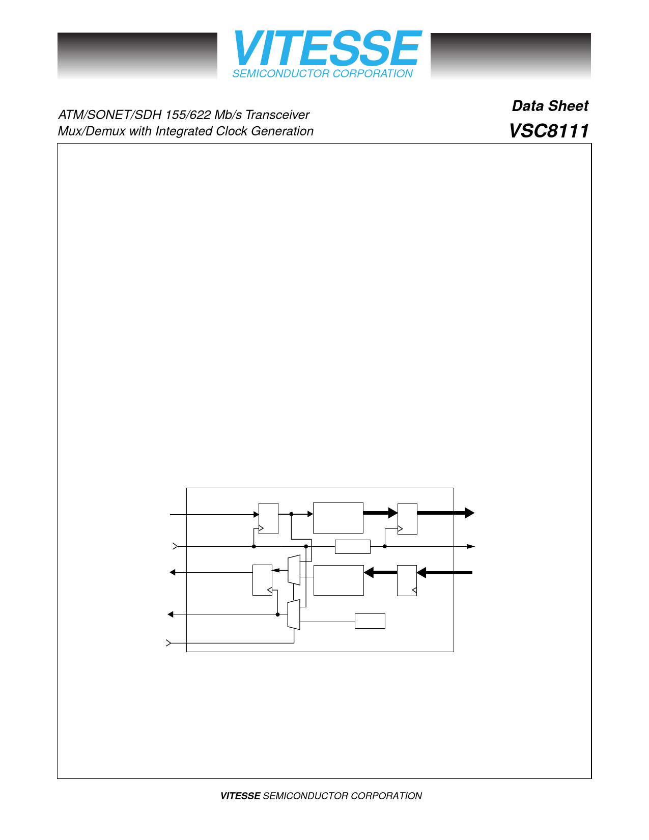
Facility Loopback
The Facility Loopback function is controlled by the FACLOOP signal. When the FACLOOP signal is set
high, the Facility Loopback mode is activated and the high speed serial receive data (RXDATAIN) is presented
at the high speed transmit output (TXDATAOUT). See Figure 3. In addition, the high speed receive clock input
(RXCLKIN) is selected and presented at the high speed transmit clock output (TXCLKOUT). In Facility Loop-
back mode the high speed receive data (RXDATAIN) is also converted to parallel data and presented at the low
speed receive data output pins (RXOUT [7:0]). The receive clock (RXCLKIN) is also divided down and pre-
sented at the low speed clock output (RXLSCKOUT).
Figure 3: Facility Loopback Data Path
RXDATAIN
RXCLKIN
TXDATAOUT
TXCLKOUT
FACLOOP
DQ
1
QD
0
1
0
1:8
Serial to
Parallel
÷8
8:1
Parallel to
Serial
DQ
QD
PLL
RXOUT[7:0]
RXLSCKOUT
TXIN[7:0]
Equipment Loopback
The Equipment Loopback function is controlled by the EQULOOP signal. When the EQULOOP signal is
set high, the Equipment Loopback mode is activated and the high speed transmit data generated from the paral-
Page 4
© VITESSE SEMICONDUCTOR CORPORATION
741 Calle Plano, Camarillo, CA 93012 • 805/388-3700 • FAX: 805/987-5896
G52142-0, Rev 4.2
8/31/98
Share Link: