VSC8116 查看數據表(PDF) - Vitesse Semiconductor
零件编号
产品描述 (功能)
生产厂家
VSC8116
Vitesse Semiconductor

VSC8116 Datasheet PDF : 20 Pages
| |||
Data Sheet
VSC8116
VITESSE
SEMICONDUCTOR CORPORATION
ATM/SONET/SDH 622/155Mb/s Transceiver
Mux/Demux with Integrated Clock Generation
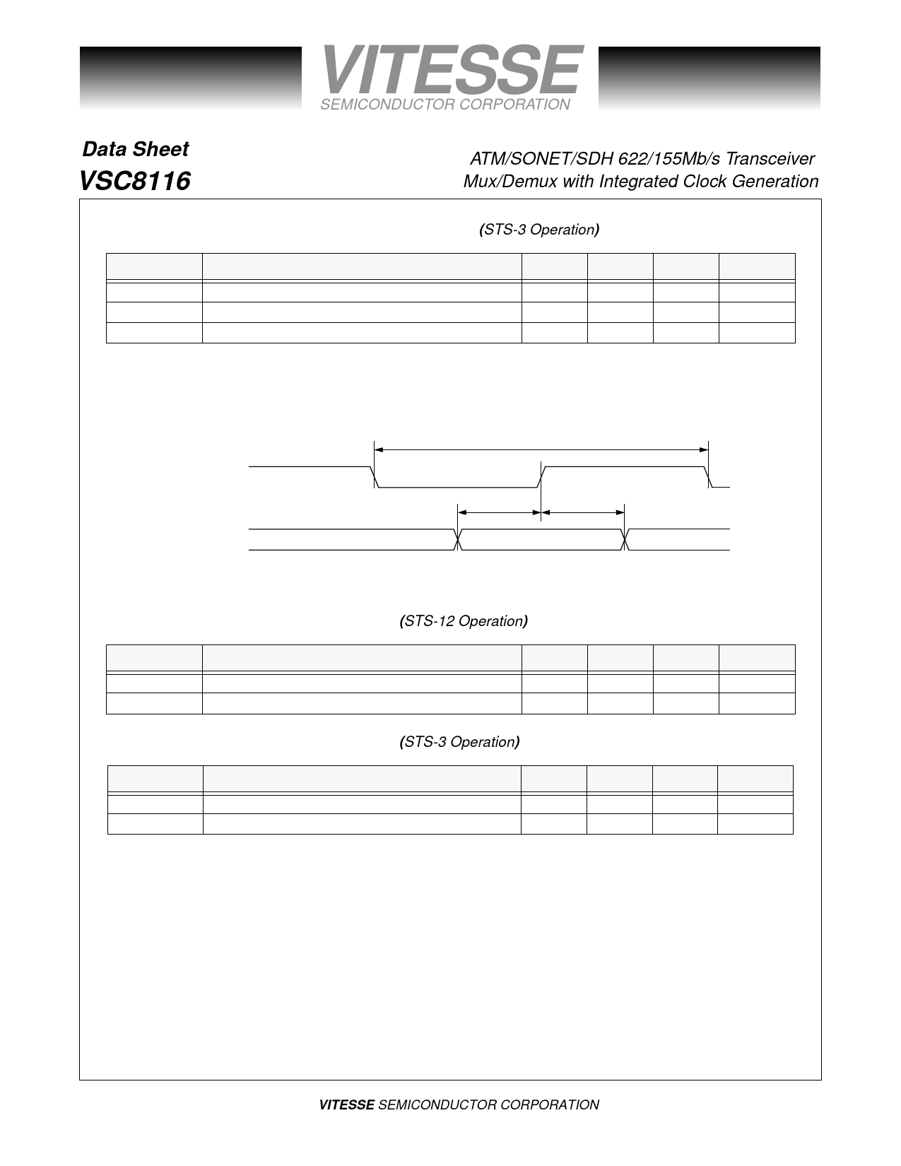
Table 5: Receive High Speed Data Input Timing Table (STS-3 Operation)
Parameter
TRXCLK
TRXSU
TRXH
Description
Receive clock period
Serial data setup time with respect to RXCLKIN
Serial data hold time with respect to RXCLKIN
Min
Typ
-
6.43
1.5
-
1.5
-
Figure 8: Transmit Data Input Timing Diagram
Max
-
-
-
Units
ns
ns
ns
TXLSCKOUT
TXIN [7:0]
TCLKOUT
TINSU
TINH
Table 6: Transmit Data Input Timing Table (STS-12 Operation)
Parameter
Description
Min
Typ
Max
Units
TINSU
Transmit data setup time with respect to TXLSCKOUT
1.0
-
-
ns
TINH
Transmit data hold time with respect to TXLSCKOUT
1.0
-
-
ns
Table 7: Transmit Data Input Timing Table (STS-3 Operation)
Parameter
Description
Min
Typ
Max
Units
TINSU
Transmit data setup time with respect to TXLSCKOUT
1.0
-
-
ns
TINH
Transmit data hold time with respect to TXLSCKOUT
1.0
-
-
ns
Note: Duty cycle for TXLSCKOUT is 50% +/- 10% worst case
G52220-0, Rev 4.1
1/8/00
© VITESSE SEMICONDUCTOR CORPORATION
741 Calle Plano, Camarillo, CA 93012 • 805/388-3700 • FAX: 805/987-5896
Page 9
Share Link: