VSC8124 查看數據表(PDF) - Vitesse Semiconductor
零件编号
产品描述 (功能)
生产厂家
VSC8124 Datasheet PDF : 20 Pages
| |||
VITESSE
SEMICONDUCTOR CORPORATION
Target Specification
VSC8124
2.488 Gb/s Quad
Data Re-timer
Functional Description
Reference Clock
A clean reference clock should be provided to meet jitter specifications. An arbitrary discontinuity in refer-
ence clock phase can be tolerated without data error at slightly reduced jitter tolerance. (See Table 1) Phase
changes must not occur more often than every 20 µs. Serial data transition density must average ≥ 0.5 for that
period. Two reference clock input ports are provided. The REFSEL pin selects the active port. When REFSEL
is not driven, it floats low, selecting REFCK0. Changing REFSEL implies a phase change.
Clock Recovery
The incoming serial data on each channel is presented to a clock recovery and data re-timing circuit. For
each channel, a phase detector and low pass filter force a local clock to track the average phase of the incoming
serial data. The low pass filter is first order to prevent jitter peaking in cascaded devices.
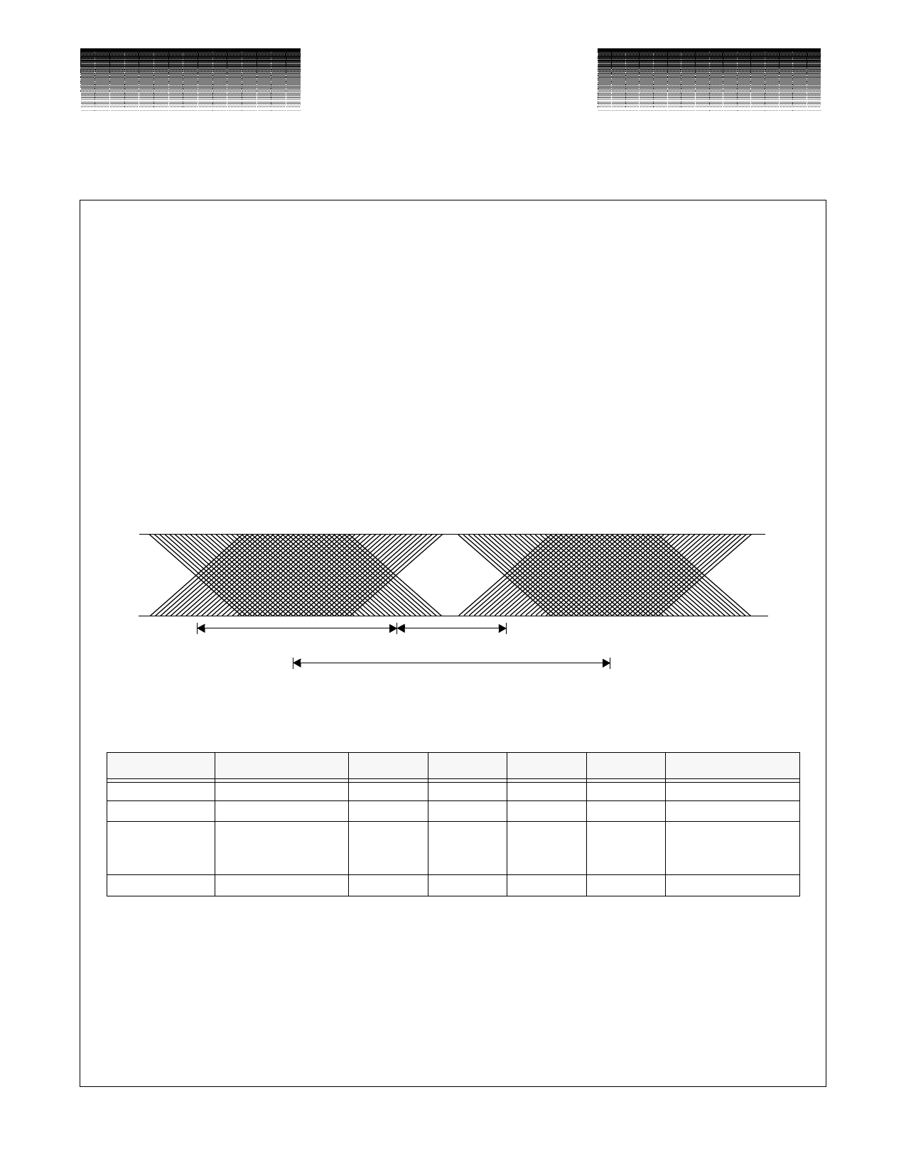
Figure 1: Serial Input Data Eye Diagram
JT
Eye Opening
Period
Table 1: Serial Input Data Specification
Parameter
JT
JT
JT
Period
Description
Jitter tolerance
Jitter tolerance
Jitter tolerance
Min
Typ
Max
Units
Conditions
220
-
-
150
170
-
190
210
-
-
401.88
-
ps
Normal Operation
ps
Fast Lock Mode
Within 20µs after
ps
REFCLK phase
change
ps
NOTE: 1) Jitter tolerance is measured at worst case power supply and temperature, using 155.52 MHz clean reference clock
(REFCK to meet 2.0 ps RMS jitter at less than 10 Mhz in bandwidth), and 600mV swing differential PRBS data
with150ps maximum rise time.
2) Jitter tolerance and re-timed data jitter are degraded in FASTLOCK mode.
3) Reference clock frequency tolerance: ∆f <= 100 ppm
4) Jitter tolerance specifications do not apply in re-timer bypass mode.
G52271-0, Rev. 1.14
2/23/00
© VITESSE SEMICONDUCTOR CORPORATION
741 Calle Plano, Camarillo, CA 93012 • 805/388-3700 • FAX: 805/987-5896
Page 3
Share Link: 