VSC8151 查看數據表(PDF) - Vitesse Semiconductor
零件编号
产品描述 (功能)
生产厂家
VSC8151 Datasheet PDF : 30 Pages
| |||
VITESSE
SEMICONDUCTOR CORPORATION
2.488Gb/s SONET/SDH
STS-48/STM-16 Section Terminator
Advance Product Information
VSC8151
SONET/SDH data is demultiplexed, framed, descrambled, and the 27 bytes of the section and line overhead are
output. The BIP parity of the incoming signal is calculated and compared with the received B1 and B2 bytes for
calculating received parity errors. The byte aligned data, calculated B1/B2 parity, and frame boundary location
are then passed to the modification section where new overhead bytes are inserted. The modified data is
rescrambled, and B1/B2 parity recalculated (if desired) prior to serialization and output. An internal state
machine generates a section alarm inhibit signal (AIS) with user defined transport overhead that can be alterna-
tively transmitted in place of the received signal.
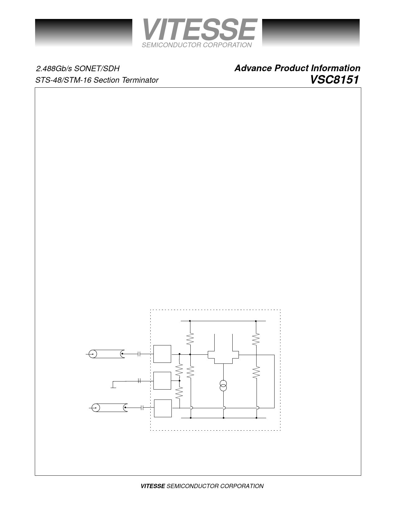
2.5G Serial and Parallel Input Interfaces
The demux receives differential clock and data signals at the appropriate SONET/SDH rate and demulti-
plexes the data for framing. These inputs are internally terminated by a center-tapped resistor network and
include biasing resistors to facilitate AC coupling. For differential input DC coupling, the network is terminated
to the appropriate termination voltage VTerm providing a 50Ω to VTerm termination for both true and complement
inputs. For differential input AC coupling, the network is terminated to VTerm via a blocking capacitor.
The common mode reference voltage is created by a resistor divider as shown. If the input signal is driven
differentially and DC-coupled to the part, the mid-point of the input signal swing should be centered about this
reference voltage and not exceed the maximum allowable amplitude. For single-ended, DC-coupling operations,
it is recommended that the user provides an external reference voltage which has better temperature and power
supply noise rejection than the on-chip resistor divider. The external reference should have a nominal value
equivalent to the common mode switch point of the DC coupled signal, and can be connected to either side of
the differential gate.
Figure 1: High Speed Serial Clock and Data Inputs
Chip Boundary
VCC = 3.3V
ZO
CIN
CAC
VTERM
CSE
ZO
50Ω
50Ω
1.65V
1.65V
VEE = 0V
CIN TYP = 100 pF (clock), 100nF (data)
CSE TYP = 100 pF (clock), 100nF (data) for single ended applications.
R | | = 1.5kΩ
Page 2
© VITESSE SEMICONDUCTOR CORPORATION
741 Calle Plano, Camarillo, CA 93012 • 805/388-3700 • FAX: 805/987-5896
G52225-0, Rev. 2.9
12/1/99
Share Link: 