VSC8151 查看數據表(PDF) - Vitesse Semiconductor
零件编号
产品描述 (功能)
生产厂家
VSC8151 Datasheet PDF : 30 Pages
| |||
VITESSE
SEMICONDUCTOR CORPORATION
2.488Gb/s SONET/SDH
STS-48/STM-16 Section Terminator
Advance Product Information
VSC8151
The serial mux output can be bypassed and the 16-bit single-ended PECL bus TXPOUT[15:0] can be used
to output modified SONET/SDH data or AIS to another device. These outputs are enabled by setting the DP bit
in the MISC register appropriately, and should be disabled if not being used. It is possible to use both the 16-bit
parallel output bus and the 2.5Gb/s serial output simultaneously. The POUTCLK output is used to provide a bus
output clock for RXFPOUT and is a divide-by-16 version of TXSCLKIN.
2.5G Output Clocking Domains
The 2.5GHz clock input to the VSC8151 mux (TXSCLKIN) acts as the permanent transmit clock for the
VSC8151. An internal clock domain boundary exists between the monitor and the transmit sections of the
device, allowing the AIS transmit portion to function completely independently of the receive portion. This
allows a CDR to track whatever data is being received and allows the VSC8151 to monitor in-frame status of
the signal continuously.
During a LOS condition, the CDR clock output may drift outside of the SONET/SDH transmission stan-
dard of +/-20PPM. By providing the option of using an external clock multiplication unit (CMU), one can
maintain a standard of +/-20PPM even during AIS states. This backup CMU receives it’s timing reference from
either a local AIS reference or the divided clock from the received RXSCLKIN +/-, depending whether AIS
transmit mode is selected or not.
The user controls the source of the reference clock output through settings in the VSC8151 register file.
The user will change these settings at the same time AIS is asserted or when imminent loss of RXSCLKIN
clock quality exists. The AIS reference output can be switched from a divided down RXSCLKIN signal to a
copy of one of the external references, ensuring that a proper reference clock remains for the transmit multi-
plexer. (See Table 2: VSC8151 Configuration Registers, Definition 13)
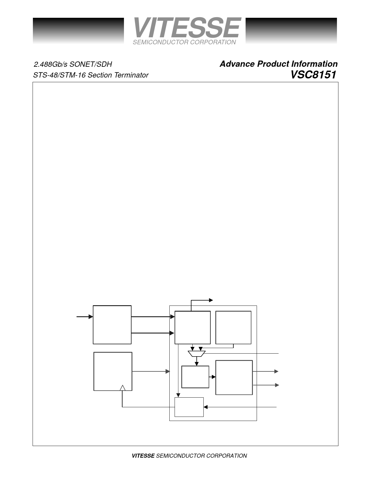
Figure 3: VSC8151 using CMU as Transmit Timing Source
Received
Data
Clock and
Data Recovery
VSC8122
RXSIN+/-
2.488Gb/s Data
622Mb/s Data
155MB/s Data
2.488GHz Clock
622MHz Clock
155MHz Clock
RXSCLKIN+/-
SEF/LOF ALARMS
Demux &
Monitor
Logic
AIS State
Machine
AIS Insert
Clock
Multiplication
Unit
VSC812X
TXSCLKIN+/-
2.488GHz Clock
622MHz Clock
155MHz Clock
AIS Reference
78 MHz
Modify
Logic
CMU
Reference
Generator
Mux &
Frame
Assembly
Logic
TXSOUT+/-
TXSCLKOUT+/-
AIS Reference
155/78 MHz
Page 4
© VITESSE SEMICONDUCTOR CORPORATION
741 Calle Plano, Camarillo, CA 93012 • 805/388-3700 • FAX: 805/987-5896
G52225-0, Rev. 2.9
12/1/99
Share Link: 