VSC8169QR 查看數據表(PDF) - Vitesse Semiconductor
零件编号
产品描述 (功能)
生产厂家
VSC8169QR Datasheet PDF : 18 Pages
| |||
VITESSE
SEMICONDUCTOR CORPORATION
OC-48 (FEC) 16:1 SONET/SDH
MUX with Clock Generator
Preliminary Data Sheet
VSC8169
Functional Description
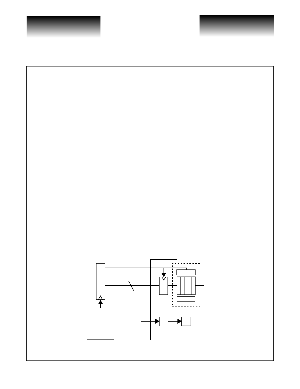
Low-Speed Interface
The Upstream Device should use the CLK16O as the timing source for its final output latch (see Figure 1).
The Upstream Device should then generate a CLK16I that is phase aligned with the data. The VSC8169 will
latch D[15:0]± on the rising edge of CLK16I+. The data must meet setup and hold times with respect to
CLK16I (see Table 2). In addition to the CLK16O clock output, there also exists a utility REFCLKO output sig-
nal, which is a clock with the same rate as that presented at the REFCLK input.
A FIFO exists within the VSC8169 to eliminate difficult system loop timing issues. Once the PLL has
locked to the reference clock, RESET must be held low for a minimum of five CLK16 cycles to initialize the
FIFO, then RESET should be set high and held constant for continuous FIFO operation. For the transparent
mode of operation (no FIFO), simply hold RESET at a constant low state (see Figure 2).
The use of a FIFO permits the system designer to tolerate an arbitrary amount of delay between CLK16O
and CLK16I. Once RESET is asserted and the FIFO initialized, the delay between CLK16O and CLK16I can
decrease or increase up to one period of the low-speed clock (6.4ns). Should this delay drift exceed one period,
the write pointer and the read pointer could point to the same word in the FIFO, resulting in a loss of transmitted
data (a FIFO overflow). In the event of a FIFO overflow, an active low FIFO_WARN signal is asserted (for a
minimum of five CLK16I cycles) which can be used to initiate a reset signal from an external controller.
The CLK16O± output driver is a LVPECL output driver designed to drive a 50Ω transmission line. The
transmission line can be DC terminated with a split-end termination scheme (see Figure 3), or DC terminated by
50Ω to VCC-2V on each line (see Figure 4). At any time, the equivalent split-end termination technique can be
substituted for the traditional 50Ω to VCC-2V on each line. AC-coupling can be achieved by a number of meth-
ods. Figure 5 illustrates an example AC-coupling method for the occasion when the downstream device pro-
vides the bias point for AC-coupling. If the downstream device were to have internal termination, the line to
line 100Ω resistor may not be necessary.
Figure 1: Low-Speed Systems Interface
Upstream
Device
CLK16I
x16
Write
16 x 5 FIFO
CLK16O
REFCLK
Read
VSC8169
2.6GHz
PLL
Divide by 16
Page 2
© VITESSE SEMICONDUCTOR CORPORATION • 741 Calle Plano • Camarillo, CA 93012
Tel: (800) VITESSE • FAX: (805) 987-5896 • Email: prodinfo@vitesse.com
Internet: www.vitesse.com
G52230-0, Rev 3.6
01/02/01
Share Link: 