W181(2000) 查看數據表(PDF) - Cypress Semiconductor
零件编号
产品描述 (功能)
生产厂家
W181 Datasheet PDF : 9 Pages
| |||
W181
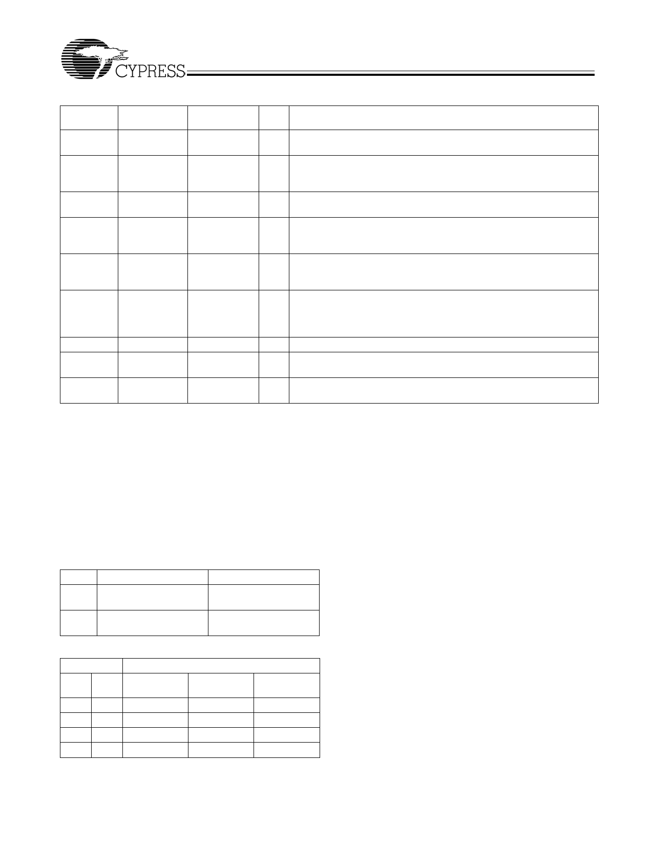
Pin Definitions
Pin Name
CLKOUT
Pin No.
(SOIC)
5
CLKIN or X1
1
Pin No.
(TSSOP)(-01)
8
2
NC or X2
SSON#
FS1:2
2
8(02/03/52/
53)
7, 8 (01/51)
3
--
12, 1
SS%
4
6
VDD
GND
NC
6
10
3
4
5, 7, 9, 11, 13,
14
Pin
Type
O
I
I
I
I
I
P
G
NC
Pin Description
Output Modulated Frequency: Frequency modulated copy
of the unmodulated input clock (SSON# asserted).
Crystal Connection or External Reference Frequency In-
put: This pin has dual functions. It may either be connected
to an external crystal, or to an external reference clock.
Crystal Connection: If using an external reference, this pin
must be left unconnected.
Spread Spectrum Control (Active LOW): Asserting this sig-
nal (active LOW) turns the internal modulation waveform on.
This pin has an internal pull-down resistor.
Frequency Selection Bit(s) 1 and 2: These pins select the
frequency range of operation. Refer to Table 2. These pins
have internal pull-up resistors.
Modulation Width Selection: When Spread Spectrum fea-
ture is turned on, this pin is used to select the amount of
variation and peak EMI reduction that is desired on the output
signal. This pin has an internal pull-up resistor.
Power Connection: Connected to 3.3V or 5V power supply.
Ground Connection: Connect all ground pins to the com-
mon system ground plane.
No Connection.
2
Share Link: 