W91312N 查看數據表(PDF) - Winbond
零件编号
产品描述 (功能)
生产厂家
W91312N Datasheet PDF : 11 Pages
| |||
Preliminary W91312N
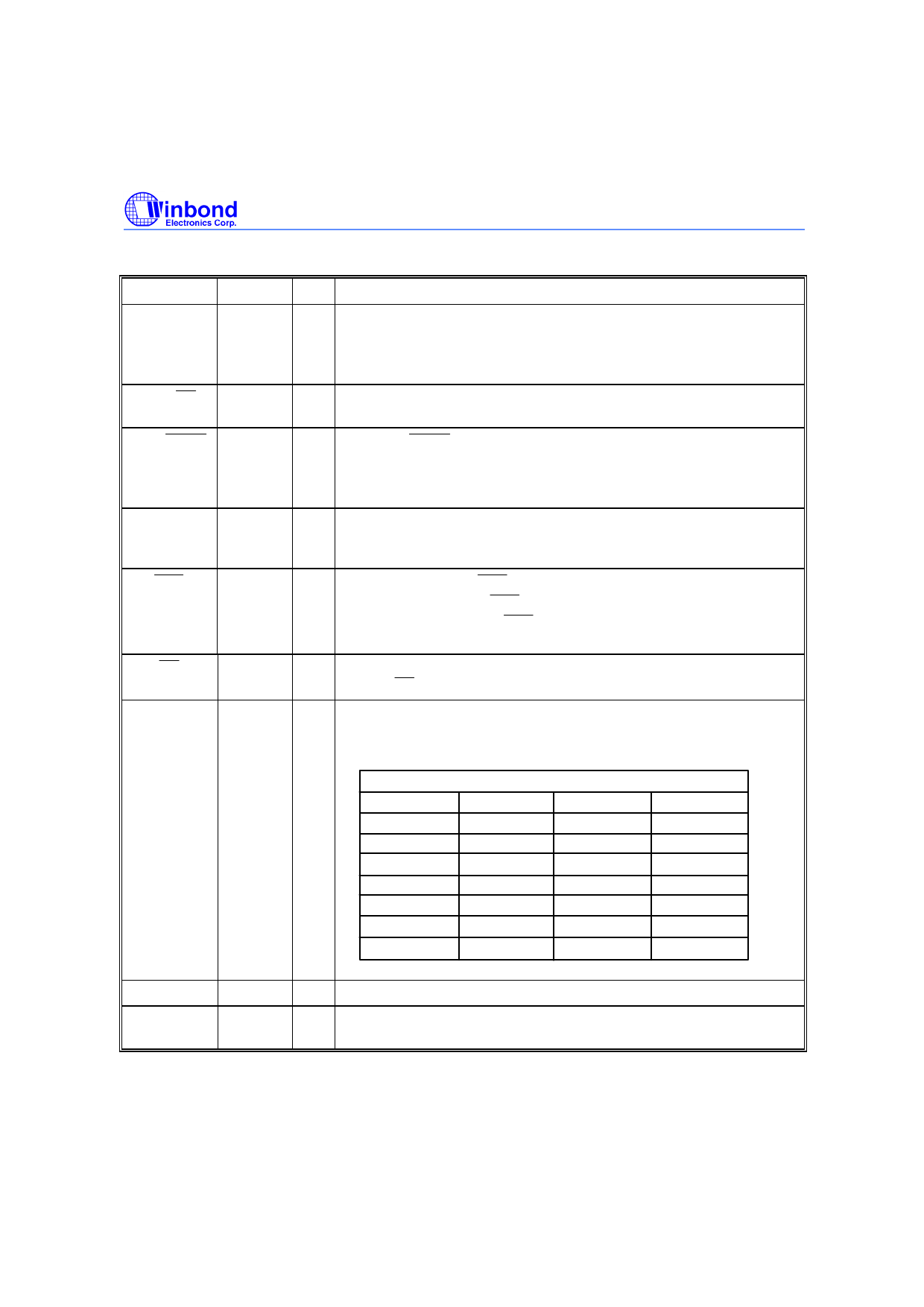
PIN DESCRIPTION
SYMBOL
Column-
Row Inputs
PIN
1−4
&
15−18
XT, XT
7, 8
T/P MUTE
9
MODE
13
HKS
10
DP
11
DTMF
12
I/O
FUNCTION
I The keyboard input may be from either the standard 4 × 4
keyboard or an inexpensive single contact (form A) keyboard.
Electronic input from a µC can also be used. A valid key entry is
defined as a single row being connected to a single column.
I, O A built-in inverter provides oscillation with an inexpensive
3.579545 MHz crystal or ceramic resonator.
O The T/P MUTE is a conventional CMOS N-channel open drain
output. The output transistor is switched on during pulse and tone
mode dialing sequence and flash break. Otherwise, it is switched
off.
I Pulling mode pin to VSS places the dialer in tone mode. Pulling
mode pin to VDD places the dialer in pulse mode (10 ppS). Leaving
mode pin floating places the dialer in pulse mode (20 ppS).
I Hook switch input. HKS = 1: On-hook state. Chip in sleeping
mode, no operation. HKS = 0: Off-hook state. Chip enabled for
normal operation. The HKS pin is pulled to VDD by an internal
resistor.
O N-channel open drain dialing pulse output (Figure 1). Flash key will
cause DP to go active in both pulse mode and tone mode.
O In pulse mode, remains in low state at all times. In tone mode,
outputs a dual or single tone. Detailed timing diagram for tone
mode is shown in Figure 2(a, b).
OUTPUT FREQUENCY
Specified
Actual
Error %
R1
697
699
+0.28
R2
770
766
-0.52
R3
852
848
-0.47
R4
941
948
+0.74
C1
1209
1216
+0.57
C2
1336
1332
-0.30
C3
1477
1472
-0.34
VDD, VSS
B/M
14, 6
5
I Power input pins.
I The break make ratio is 60:40 if B/M = 1 and is 66.6:33.3 if B/M =
0. This pin has no function in DTMF mode.
-2-
Share Link: 