WED3EG7233S-D3 查看數據表(PDF) - White Electronic Designs Corporation
零件编号
产品描述 (功能)
生产厂家
WED3EG7233S-D3 Datasheet PDF : 11 Pages
| |||
White Electronic Designs
WED3EG7233S-D3
-JD3
ADVANCED
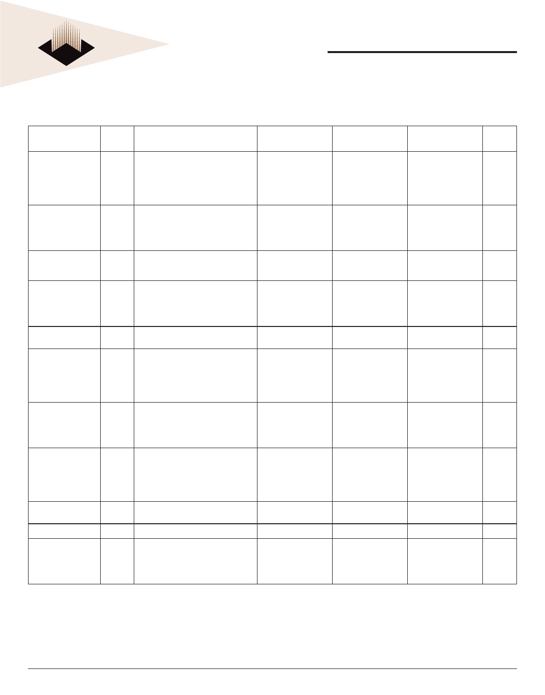
IDD SPECIFICATIONS AND TEST CONDITIONS
Recommended operating conditions, 0°C ≤ TA ≤ 70°C, VCCQ = 2.5V ± 0.2V, VCC = 2.5V ± 0.2V
Includes DDR SDRAM component only
Parameter
Symbol Conditions
Operating Current
IDD0 One device bank; Active - Precharge;
tRC=tRC (MIN); tCK=tCK (MIN); DQ,DM
and DQS inputs changing once per
clock cycle; Address and control
inputs changing once every two
cycles.
Operating Current
IDD1 One device bank; Active-Read-
Precharge Burst = 2; tRC=tRC (MIN);
tCK=tCK (MIN); lOUT = 0mA; Address
and control inputs changing once per
clock cycle.
Precharge Power-
Down Standby
Current
IDD2P All device banks idle; Power-down
mode; tCK=tCK (MIN); CKE=(low)
Idle Standby Current IDD2F CS# = High; All device banks idle;
tCK=tCK (MIN); CKE = high; Address
and other control inputs changing
once per clock cycle. VIN = VREF for
DQ, DQS and DM.
Active Power-Down
Standby Current
IDD3P One device bank active; Power-Down
mode; tCK (MIN); CKE=(low)
Active Standby
Current
IDD3N CS# = High; CKE = High; One device
bank; Active-Precharge; tRC=tRAS
(MAX); tCK=tCK (MIN); DQ, DM and
DQS inputs changing twice per clock
cycle; Address and other control
inputs changing once per clock cycle.
Operating Current
IDD4R Burst = 2; Reads; Continuous burst;
One device bank active; Address
and control inputs changing once
per clock cycle; TCK= TCK (MIN); lOUT
= 0mA.
Operating Current
IDD4W Burst = 2; Writes; Continuous burst;
One device bank active; Address
and control inputs changing once per
clock cycle; tCK=tCK (MIN); DQ,DM
and DQS inputs changing once per
clock cycle.
Auto Refresh
Current
IDD5 tRC = tRC (MIN)
Self Refresh Current IDD6 CKE ≤ 0.2V
Operating Current
IDD7A Four bank interleaving Reads (BL=4)
with auto precharge with tRC=tRC
(MIN); tCK=tCK (MIN); Address and
control inputs change only during
Active Read or Write commands.
DDR266@CL=2.0
Max
TBD
TBD
TBD
TBD
TBD
TBD
TBD
TBD
TBD
TBD
TBD
DDR266@CL=2.5
Max
1845
2205
72
810
450
900
2250
2115
3015
72
4050
DDR200@CL=2
Max
1845
2205
72
810
450
900
2250
2115
3015
72
4050
Units
mA
mA
rnA
mA
mA
mA
mA
rnA
mA
mA
mA
White Electronic Designs Corp. reserves the right to change products or specifications without notice.
May, 2005
Rev. 0
5
White Electronic Designs Corporation • (602) 437-1520 • www.wedc.com
Share Link: 