WFW9N90W 查看數據表(PDF) - Shenzhen Winsemi Microelectronics Co., Ltd
零件编号
产品描述 (功能)
生产厂家
WFW9N90W Datasheet PDF : 7 Pages
| |||
Features
■ 9A,900V, RDS(on)(Max1.35Ω)@VGS=10V
■ Ultra-low Gate charge(Typical 58nC)
■ Fast Switching Capability
■ 100%Avalanche Tested
■ Maximum Junction Temperature Range(150℃)
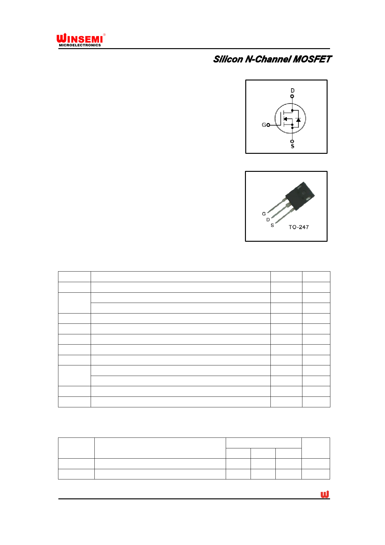
WFW9N90W
Silicon N-Channel MOSFET
General Description
This N-Channel enhancement mode power field effect
transistors are produced using Winsemi's proprietary, planar
stripe ,DMOS technology. This advanced technology has
been especially tailored to minimize on-state resistance,
provide superior switching performance, and withstand high
energy pulse in the avalanche and commutation mode. These
devices are well suited for high efficiency switch mode power
supplies.
Absolute Maximum Ratings
Symbol
Parameter
VDSS
ID
Drain Source Voltage
Continuous Drain Current(@Tc=25℃)
Continuous Drain Current(@Tc=100℃)
IDM
Drain Current Pulsed
VGS
Gate to Source Voltage
EAS
Single Pulsed Avalanche Energy
EAR
Repetitive Avalanche Energy
dv/dt
Peak Diode Recovery dv /dt
Total Power Dissipation(@Tc=25℃)
PD
Derating Factor above 25℃
TJ,Tstg
Junction and Storage Temperature
TL
Channel Temperature
(Note1)
(Note2)
(Note1)
(Note3)
Value
900
9
5.7
27
±30
663
15
4.5
68
0.54
-55~150
300
Units
V
A
A
A
V
mJ
mJ
V/ ns
W
W/℃
℃
℃
Thermal Characteristics
Symbol
Parameter
RQJC
RQJA
Thermal Resistance , Junction -to -Case
Thermal Resistance , Junction-to -Ambient
Value
Min Typ Max
-
-
1.85
-
-
62.5
Units
℃/W
℃/W
Rev.A Oct.2010
Copyright@Winsemi Microelectronics Co., Ltd., All right reserved.
Share Link: 