ICX249AK 查看數據表(PDF) - Sony Semiconductor
零件编号
产品描述 (功能)
生产厂家
ICX249AK Datasheet PDF : 21 Pages
| |||
ICX249AK
Bias Conditions 1 [when used in substrate bias internal generation mode]
Item
Symbol Min.
Typ.
Max. Unit Remarks
Output circuit supply voltage
VDD
14.55
15.0
15.45
V
Reset drain voltage
VRD
14.55
15.0
15.45
V VRD = VDD
Output circuit gate voltage
Output circuit source
Protective transistor bias
VGG
1.75
2.0
2.25
V
VSS
Grounded with 390Ω resistor
VL
∗1
Substrate bias circuit supply voltage
Substrate clock
VDSUB
φSUB
14.55
15.0
∗2
15.45
V
∗1 VL setting is the VVL voltage of the vertical transfer clock waveform, or the same supply voltage as the VL
power supply for the V driver should be used. (When CXD1267AN is used.)
∗2 Do not apply a DC bias to the substrate clock pin, because a DC bias is generated within the CCD.
Bias Conditions 2 [when used in substrate bias external adjustment mode]
Item
Symbol Min.
Typ.
Max. Unit Remarks
Output circuit supply voltage
VDD
14.55
15.0
15.45
V
Reset drain voltage
VRD
14.55
15.0
15.45
V VRD = VDD
Output circuit gate voltage
VGG
1.75
2.0
2.25
V
Output circuit source
Protective transistor bias
Substrate bias circuit supply voltage
Substrate voltage adjustment range
Substrate voltage adjustment precision
VSS
VL
VDSUB
VSUB
∆VSUB
Grounded with 390Ω resistor
∗3
∗4
6.0
14.0
–3
+3
V ∗5
% ∗5
∗3 VL setting is the VVL voltage of the vertical transfer clock waveform, or the same supply voltage as the VL
power supply for the V driver should be used. (When CXD1267AN is used.)
∗4 Connect to GND or leave open.
∗5 The setting value of the substrate voltage (VSUB) is indicated on the back of the image sensor by a special
code. When adjusting the substrate voltage externally, adjust the substrate voltage to the indicated voltage.
The adjustment precision is ±3%. However, this setting value has not significance when used in substrate
bias internal generation mode.
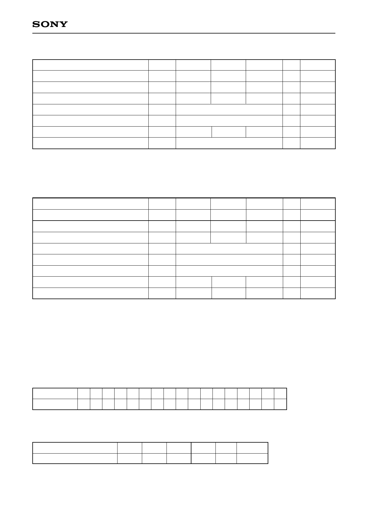
VSUB code — one character indication
Code and optimal setting correspond to each other as follows.
VSUB code
E f G h J K L mNP QR S T U VW
Optimal setting 6.0 6.5 7.0 7.5 8.0 8.5 9.0 9.5 10.0 10.5 11.0 11.5 12.0 12.5 13.0 13.5 14.0
<Example> "L" → VSUB = 9.0V
DC Characteristics
Item
Symbol Min.
Output circuit supply current IDD
Typ. Max.
5.0 10.0
–4–
Unit Remarks
mA
Share Link: 