XM28C040 查看數據表(PDF) - Xicor -> Intersil
零件编号
产品描述 (功能)
生产厂家
XM28C040 Datasheet PDF : 17 Pages
| |||
XM28C040
PIN DESCRIPTIONS
Addresses (A0–A18)
The Address inputs select an 8-bit memory location
during a read or write operation.
Chip Enable (CE)
The Chip Enable input must be LOW to enable all read/
write operations. When CE is HIGH, power consumption
is reduced (see Note 4).
Output Enable (OE)
The Output Enable input controls the data output buffers
and is used to initiate read operations.
Data In/Data Out (I/O0–I/O7)
Data is written to or read from the XM28C040 through
the I/O pins.
Write Enable (WE)
The Write Enable input controls the writing of data to the
XM28C040.
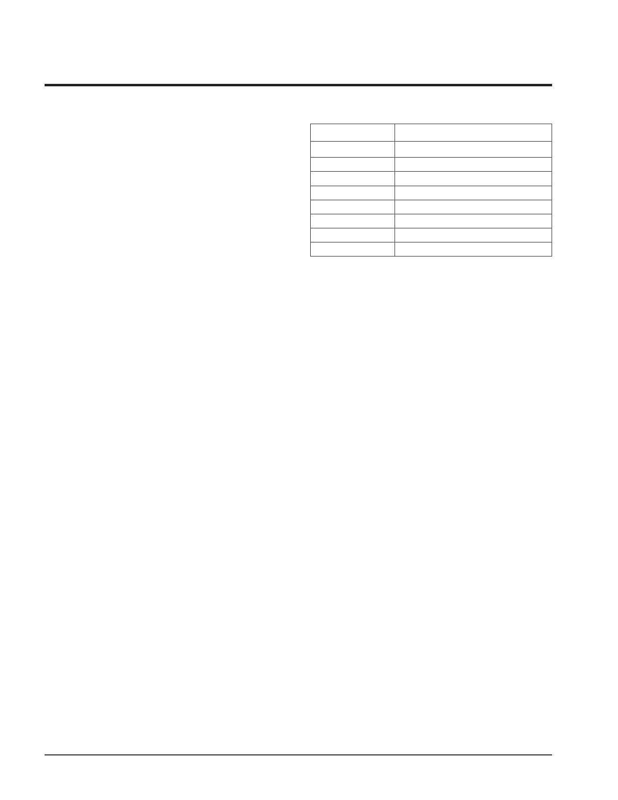
PIN NAMES
Symbol
A0–A18
I/O0–I/O8
WE
CE
OE
VCC
VSS
NC
Description
Address Inputs
Data Input/Output
Write Enable
Chip Enable
Output Enable
+5V
Ground
No Connect
3873 PGM T01
2
Share Link: 