K2411-Z 查看數據表(PDF) - NEC => Renesas Technology
零件编号
产品描述 (功能)
生产厂家
K2411-Z Datasheet PDF : 8 Pages
| |||
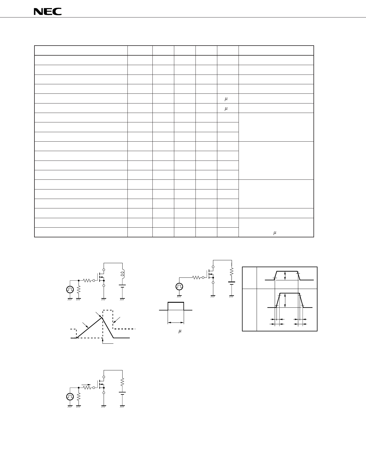
2SK2411, 2SK2411-Z
ELECTRICAL CHARACTERISTICS (TA = 25 ˚C)
CHARACTERISTIC
Drain to Source On-Resistance
Drain to Source On-Resistance
Gate to Source Cutoff Voltage
Forward Transfer Admittance
Drain Leakage Current
Gate to Source Leakage Current
Input Capacitance
Output Capacitance
Reverse Transfer Capacitance
Turn-On Delay Time
Rise Time
Turn-Off Delay Time
Fall Time
Total Gate Charge
Gate to Source Charge
Gate to Drain Charge
Body Diode Forward Voltage
Reverse Recovery Time
Reverse Recovery Charge
SYMBOL
RDS(on)1
RDS(on)2
VGS(off)
| yfs |
IDSS
IGSS
Ciss
Coss
Crss
td(on)
tr
td(off)
tf
QG
QGS
QGD
VF(S-D)
trr
Qrr
MIN.
1.0
15
TYP.
31
40
1.5
27
1500
720
190
20
260
130
150
50
5.0
15
1.1
110
320
MAX.
40
60
2.0
10
±10
UNIT
mΩ
mΩ
V
S
µA
µA
pF
pF
pF
ns
ns
ns
ns
nC
nC
nC
V
ns
nC
TEST CONDITIONS
VGS = 10 V, ID = 15 A
VGS = 4 V, ID = 15 A
VDS = 10 V, ID = 1 mA
VDS = 10 V, ID = 15 A
VDS = 60 V, VGS = 0
VGS = ±20 V, VDS = 0
VDS = 10 V
VGS = 0
f = 1 MHz
ID = 15 A
VGS(on) = 10 V
VDD = 30 V
RG = 10 Ω
ID = 30 A
VDD = 48 V
VGS = 10 V
IF = 30 A, VGS = 0
IF = 30 A, VGS = 0
di/dt = 100 A/µs
Test Circuit 1 Avalanche Capability
Test Circuit 2 Switching Time
D.U.T.
RG = 25 Ω
L
PG
50 Ω
VDD
VGS = 20 V → 0
ID
VDD
IAS BVDSS
VDS
Test Circuit 3 Gate Charge
Starting Tch
D.U.T.
PG.
RG
RG = 10 Ω
VGS
0
t
t = 1 µs
Duty Cycle ≤ 1 %
RL
VDD
VGS
Wave
Form
VGS
10 %
0
VGS (on)
ID
90 %
ID
Wave
Form
10 %
0
td (on)
ID
t t r
d (off)
90 %
90 %
10 %
tf
ton
toff
D.U.T.
IG = 2 mA
RL
PG.
50 Ω
VDD
The application circuits and their parameters are for references only and are not intended for use in actual design-in's.
2
Share Link: 