LC73861 查看數據表(PDF) - SANYO -> Panasonic
零件编号
产品描述 (功能)
生产厂家
LC73861 Datasheet PDF : 5 Pages
| |||
LC73861, LC73862
AC Electrical Characteristics at Ta = 25°C ± 2°C, VDD = 5 V, VSS = 0 V, fOSC = 4.194304 MHz
Parameter
Valid input signal level
Positive twist accept
Frequency deviation accept
Frequency deviation reject
Third tone tolerance
Dial tone tolerance
Noise tolerance
Tone present detect time
Tone absent detect time
Data shift rate
Data output delay time
Setup time delay
Data hold time
Oscillator frequency
Load capacitance
Symbol
tDP
tDA
Conditions
See notes 1, 2, 3, 5, 6 and 9.
See notes 2, 3, 4, 9 and 11.
See notes 2, 3, 5 and 9.
See notes 2, 3 and 5.
See notes 2, 3, 4, 5, 9 and 10.
See notes 2, 3, 4, 5, 8, 9 and 10.
See notes 2, 3, 4, 5, 7, 9 and 10.
See Timing Chart.
See Timing Chart.
tPAD
tDL
tDH
fOSC
CXO
See Timing Chart.
See Timing Chart.
See Timing Chart.
LC73861
LC73862
OSCI and OSCO
Notes
1. 0 dBm = 1 mW power when driving a 600 Ω load.
2. All 16 DTMF signal frequencies.
3. 40 ms DTMF signal period and 40 ms pause period.
4. Nominal DTMF frequency.
5. Low-frequency group and High-frequency group signal levels are the same.
6. DTMF signal frequency deviation is within ±1.5% ±2 Hz.
7. Bandwidth limited (0 to 3 kHz) Gaussian noise.
8. 350 Hz and 440 Hz dial tone frequencies.
9. Error rate of less than 1 in 10,000.
10. Referenced to the lowest frequency component of the DTMF signal.
11. Twist = High-frequency group tone level ÷ Low-frequency group tone level.
min
typ
max
–49.5
0
6
±1.5% ±2
±3.5
–16
22
–12
3
20
0.5
20
1
100
0
30
4.190109 4.194304 4.198498
3.5759 3.5795 3.5831
30
Unit
dBm
dB
Hz
%
dB
dB
dB
ms
ms
MHz
ns
ns
ns
MHz
MHz
pF
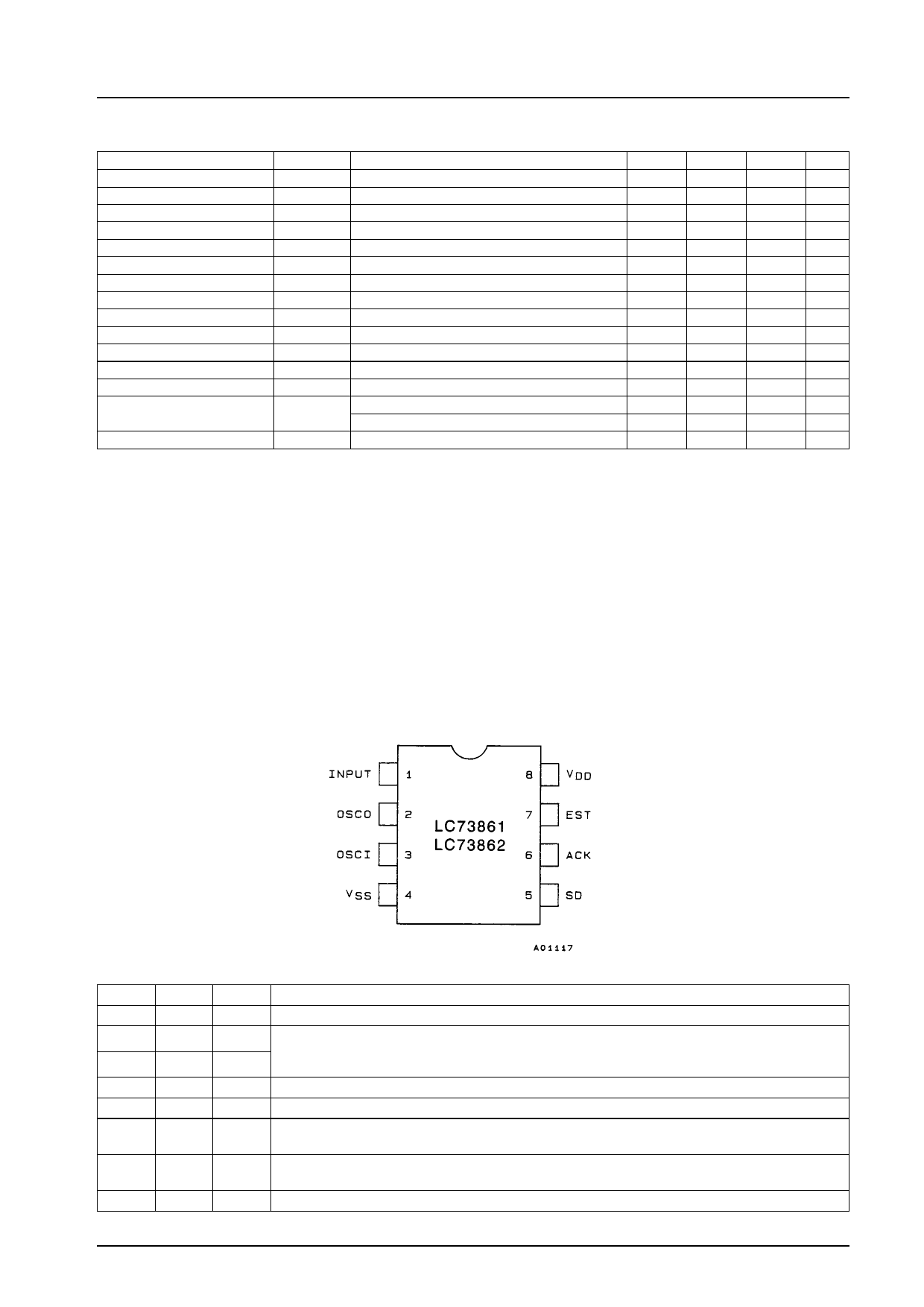
Pin Assignment
Pin Description
Top view
Number
1
2
Name
INPUT
OSCO
3
OSCI
4
VSS
5
SD
6
ACK
7
EST
8
VDD
I/O
Description
I
Input coupling capacitor required. Biased internally to VDD/2.
O An oscillating circuit is formed by connecting a 4.194304 MHz (LC73861) / 3.579545 MHz (LC73826)
oscillator and a capacitor (if needed) between these pins. (To determine whether an external
I
capacitor is needed or not, contact the manufacturer of the oscillator.)
Supply pin, normally 0 V
O Outputs 4-bit serial decoded DTMF output, least significant bit first.
I
The ACK pin is used to shift out data to the SD pin. Four pulses are needed in order to shift out the
4-bit DTMF code. The data is latched by the shift register before the rising edge of the first pulse.
O Indicates the presence of a DTMF signal when HIGH. (This pin can be monitored and after a short
delay, data can be accessed by 4 pulses to ACK.)
O Supply pin, normally 4.5 V to 5.5 V
No.4431-2/5
Share Link: 