74VHC139MTC 查看數據表(PDF) - Fairchild Semiconductor
零件编号
产品描述 (功能)
生产厂家
74VHC139MTC Datasheet PDF : 6 Pages
| |||
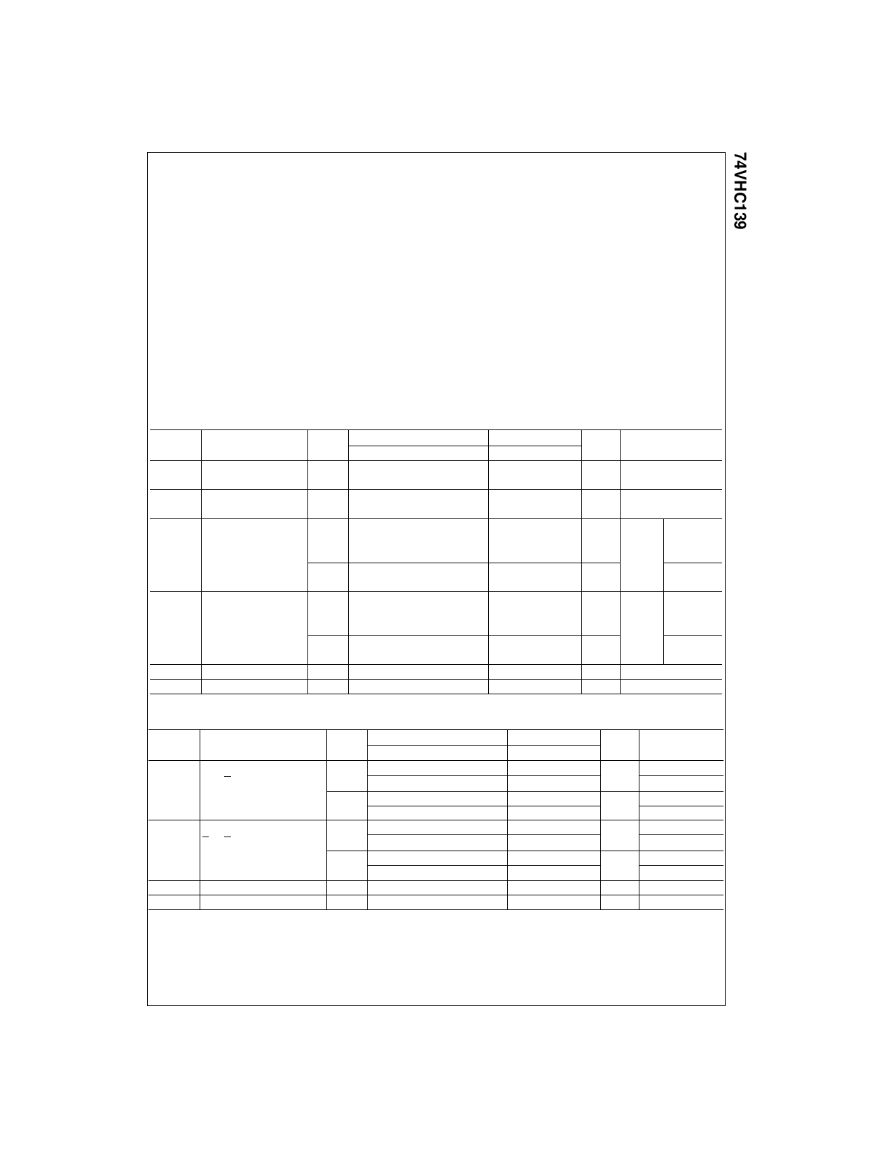
Absolute Maximum Ratings(Note 1)
Supply Voltage (VCC)
DC Input Voltage (VIN)
DC Output Voltage (VOUT)
Input Diode Current (IIK)
Output Diode Current (IOK)
DC Output Current (IOUT)
DC VCC/GND Current (ICC)
Storage Temperature (TSTG)
Lead Temperature (TL)
(Soldering, 10 seconds)
−0.5V to +7.0V
−0.5V to +7.0V
−0.5V to VCC + 0.5V
−20 mA
±20 mA
±25 mA
±75 mA
−65°C to +150°C
260°C
Recommended Operating
Conditions (Note 2)
Supply Voltage (VCC)
2.0V to +5.5V
Input Voltage (VIN)
0V to +5.5V
Output Voltage (VOUT)
0V to VCC
Operating Temperature (TOPR)
−40°C to +85°C
Input Rise and Fall Time (tr, tf)
VCC = 3.3V ± 0.3V
0 ∼ 100 ns/V
VCC = 5.0V ± 0.5V
0 ∼ 20 ns/V
Note 1: Absolute Maximum Ratings are values beyond which the device
may be damaged or have its useful life impaired. The databook specifica-
tions should be met, without exception, to ensure that the system design is
reliable over its power supply, temperature, and output/input loading vari-
ables. Fairchild does not recommend operation outside databook specifica-
tions.
Note 2: Unused inputs must be held HIGH or LOW. They may not float.
DC Electrical Characteristics
Symbol
VIH
VIL
VOH
VOL
IIN
ICC
Parameter
VCC
(V)
HIGH Level
2.0
Input Voltage
3.0 − 5.5
LOW Level
2.0
Input Voltage
3.0 − 5.5
HIGH Level
2.0
Output Voltage
3.0
4.5
3.0
4.5
LOW Level
2.0
Output Voltage
3.0
4.5
3.0
4.5
Input Leakage Current
0 − 5.5
Quiescent Supply Current 5.5
Min
1.50
0.7 VCC
1.9
2.9
4.4
2.58
3.94
TA = 25°C
Typ
2.0
3.0
4.5
0.0
0.0
0.0
Max
0.50
0.3 VCC
0.1
0.1
0.1
0.36
0.36
±0.1
4.0
TA = −40°C to +85°C
Min
Max
1.50
0.7 VCC
0.50
0.3 VCC
1.9
2.9
4.4
2.48
3.80
0.1
0.1
0.1
0.44
0.44
±1.0
40.0
Units
Conditions
V
V
VIN = VIH IOH = −50 µA
V
or VIL
V
IOH = −4 mA
IOH = −8 mA
VIN = VIH IOL = 50 µA
V
or VIL
V
IOL = 4 mA
IOL = 8 mA
µA VIN = 5.5V or GND
µA VIN = VCC or GND
AC Electrical Characteristics
Symbol
Parameter
VCC
TA = 25°C
TA = −40°C to +85°C
Units
Conditions
(V)
Min
Typ
Max
Min
Max
tPLH
Propagation Delay
tPHL
An to On
3.3 ± 0.3
7.2
11.0
1.0
13.0
ns CL = 15 pF
9.7
14.5
1.0
16.5
CL = 50 pF
5.0 ± 0.5
5.0
7.2
1.0
8.5
ns CL = 15 pF
6.5
9.2
1.0
10.5
CL = 50 pF
tPLH
Propagation Delay
tPHL
En to On
3.3 ± 0.3
6.4
9.2
1.0
11.0
ns CL = 15 pF
8.9
12.7
1.0
14.5
CL = 50 pF
5.0 ± 0.5
4.4
6.3
1.0
7.5
ns CL = 15 pF
5.9
8.3
1.0
9.5
CL = 50 pF
CIN
Input Capacitance
4
10
10
pF VCC = Open
CPD
Power Dissipation Capacitance
26
pF (Note 3)
Note 3: CPD is defined as the value of the internal equivalent capacitance which is calculated from the operating current consumption without load. Average
operating current can be obtained by the equation: ICC (opr.) = CPD * VCC * fIN + ICC/2 (per decoder).
3
www.fairchildsemi.com
Share Link: 