TISP1072F3SL 查看數據表(PDF) - Power Innovations
零件编号
产品描述 (功能)
生产厂家
TISP1072F3SL Datasheet PDF : 17 Pages
| |||
TISP1072F3, TISP1082F3
DUAL ASYMMETRICAL TRANSIENT
VOLTAGE SUPPRESSORS
SEPTEMBER 1993 - REVISED SEPTEMBER 1997
description (continued)
These monolithic protection devices are fabricated in ion-implanted planar structures to ensure precise and
matched breakover control and are virtually transparent to the system in normal operation
The small-outline 8-pin assignment has been carefully chosen for these devices to maximise the inter-pin
clearance and creepage distances which are used by standards (e.g. IEC950) to establish voltage withstand
ratings.
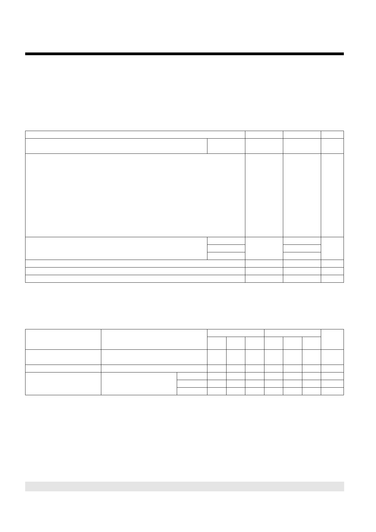
absolute maximum ratings
RATING
Repetitive peak off-state voltage ( 0°C < TJ <70°C)
‘1072F3
‘1082F3
Non-repetitive peak on-state pulse current (see Notes 1, 2 and 3)
1/2 µs (Gas tube differential transient, open-circuit voltage wave shape 1/2 µs)
2/10 µs (FCC Part 68, open-circuit voltage wave shape 2/10 µs)
8/20 µs (ANSI C62.41, open-circuit voltage wave shape 1.2/50 µs)
10/160 µs (FCC Part 68, open-circuit voltage wave shape 10/160 µs)
5/200 µs (VDE 0433, open-circuit voltage wave shape 2 kV, 10/700 µs)
0.2/310 µs (RLM 88, open-circuit voltage wave shape 1.5 kV, 0.5/700 µs)
5/310 µs (CCITT IX K17/K20, open-circuit voltage wave shape 2 kV, 10/700 µs)
5/310 µs (FTZ R12, open-circuit voltage wave shape 2 kV, 10/700 µs)
10/560 µs (FCC Part 68, open-circuit voltage wave shape 10/560 µs)
10/1000 µs (REA PE-60, open-circuit voltage wave shape 10/1000 µs)
Non-repetitive peak on-state current (see Notes 2 and 3)
D Package
50 Hz, 1 s
P Package
SL Package
Initial rate of rise of on-state current, Linear current ramp, Maximum ramp value < 38 A
Junction temperature
Storage temperature range
SYMBOL
VDRM
ITSP
ITSM
diT/dt
TJ
Tstg
VALUE
-58
-66
UNIT
V
120
80
70
60
50
38
50
50
45
35
4
6
6
250
-40 to +150
-40 to +150
A
A rms
A/µs
°C
°C
NOTES: 1. Further details on surge wave shapes are contained in the Applications Information section.
2. Initially the TISP must be in thermal equilibrium with 0°C < TJ <70°C. The surge may be repeated after the TISP returns to its initial
conditions.
3. Above 70°C, derate linearly to zero at 150°C lead temperature.
electrical characteristics for the T and R terminals, 25°C (unless otherwise noted)
IDRM
ID
Coff
NOTE
PARAMETER
TEST CONDITIONS
TISP1072F3
MIN TYP MAX
Repetitive peak off-
state current
Off-state current
Off-state capacitance
VD = ±VDRM, 0°C < TJ <70°C
VD = ±50 V
f = 100 kHz,
VD = 0
(see Note 4)
Vd = 100 mV
D Package
P Package
SL Package
±10
±10
0.08 0.5
0.06 0.4
0.02 0.3
4: Further details on capacitance are given in the Applications Information section.
TISP1082F3
MIN TYP MAX
±10
±10
0.08 0.5
0.06 0.4
0.02 0.3
UNIT
µA
µA
pF
pF
pF
PRODUCT INFORMATION
2
Share Link: 