TISP1072F3 查看數據表(PDF) - Power Innovations
零件编号
产品描述 (功能)
生产厂家
TISP1072F3 Datasheet PDF : 17 Pages
| |||
TISP1072F3, TISP1082F3
DUAL ASYMMETRICAL TRANSIENT
VOLTAGE SUPPRESSORS
SEPTEMBER 1993 - REVISED SEPTEMBER 1997
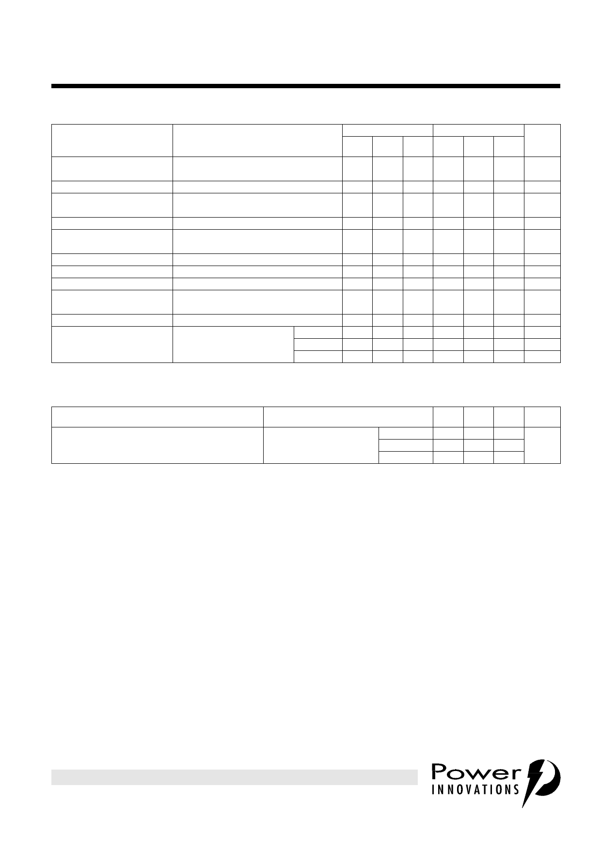
electrical characteristics for the T and G and R and G terminals, 25°C (unless otherwise noted)
IDRM
V(BO)
V(BO)
I(BO)
VFRM
VF
VT
IH
dv/dt
ID
Coff
NOTE
PARAMETER
TEST CONDITIONS
TISP1072F3
MIN TYP MAX
Repetitive peak off-
state current
VD = VDRM, 0°C < TJ <70°C
-10
Breakover voltage
dv/dt = -250 V/ms, RSOURCE = 300 Ω
Impulse breakover volt- dv/dt = -1000 V/µs, RSOURCE = 50 Ω,
age
di/dt < -20 A/µs
-72
-78
Breakover current
Peak forward recovery
voltage
Forward voltage
On-state voltage
Holding current
dv/dt = -250 V/ms, RSOURCE = 300 Ω
dv/dt = 1000 V/µs, RSOURCE = 50 Ω,
diF/dt < 20 A/µs
IT = 5 A, tW = 100 µs
IT = -5 A, tW = 100 µs
di/dt = +30 mA/ms
-0.1
-0.6
3.3
3
-3
-0.15
Critical rate of rise of Linear voltage ramp
-5
off-state voltage
Maximum ramp value < 0.85VDRM
Off-state current
VD = -50 V
-10
f = 100 kHz, Vd = 100 mV
VD = 0,
150 240
Off-state capacitance Third terminal voltage = 0
VD = -5 V
65 104
(see Note 5)
VD = -50 V
30
48
5: Further details on capacitance are given in the Applications Information section.
TISP1082F3
MIN TYP MAX
-10
-82
-92
-0.1
-0.6
3.3
3
-3
-0.15
-5
-10
130 240
55 104
25
48
UNIT
µA
V
V
A
V
V
V
A
kV/µs
µA
pF
pF
pF
thermal characteristics
PARAMETER
RθJA Junction to free air thermal resistance
TEST CONDITIONS
MIN TYP MAX UNIT
Ptot = 0.8 W, TA = 25°C
5 cm2, FR4 PCB
D Package
P Package
SL Package
160
100 °C/W
105
PRODUCT INFORMATION
3
Share Link: 