MCP6N16-001E 查看數據表(PDF) - Microchip Technology
零件编号
产品描述 (功能)
生产厂家
MCP6N16-001E Datasheet PDF : 58 Pages
| |||
MCP6N16
Minimum Gain Options
Table 1 shows key specifications that differentiate
between the different minimum gain (GMIN) options.
See Section 1.0 “Electrical Characteristics”,
Section 6.0 “Packaging Information” and Product
Identification System for further information on GMIN.
TABLE 1: KEY DIFFERENTIATING SPECIFICATIONS
Part No.
GMIN
(V/V)
Nom.
VOS
(±μV)
Max.
TC1
(±nV/°C)
Max.
TA = -40 to +125°C
CMRR
(dB)
Min.
VDD = 5.5V
PSRR
(dB)
Min.
VDMH
(V)
Min.
GBWP
(MHz)
Typ.
Eni
(μVP-P)
Typ.
f = 0.1 to 10 Hz
eni
(nV/√Hz)
Typ.
f < 500 Hz
MCP6N16-001 1 85
1800
89
91 2.7 0.50
19
900
MCP6N16-010 10 22
180
103
104 0.27 5.0
2.2
105
MCP6N16-100 100 17
60
112
110 0.027 35
0.93
45
Note 1: GMIN is the minimum stable gain (GDM), for a given part option. In other words, GDM ≥ GMIN.
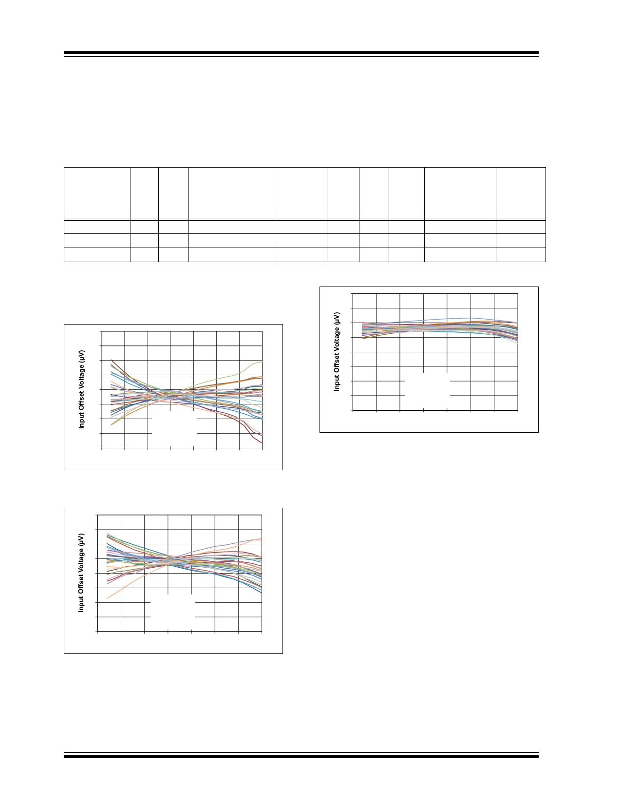
Figures 1 to 3 show input offset voltage versus
temperature for the three gain options (GMIN = 1, 10,
4
100 V/V).
3
40
30
20
10
0
-10
-20
-30
-40
-50
GMIN = 1
28 Samples
VDD = 5.5V
VCM = VDD/2
NPBW = 3 mHz
-25 0 25 50 75 100 125
Ambient Temperature (°C)
FIGURE 1:
Input Offset Voltage vs.
Temperature, with GMIN = 1.
2
1
0
-1
-2
-3
-4
-50
GMIN = 100
28 Samples
VDD = 5.5V
VCM = VDD/2
NPBW = 3 mHz
-25
0
25 50 75 100 125
Ambient Temperature (°C)
FIGURE 3:
Input Offset Voltage vs.
Temperature, with GMIN = 100.
4
3
2
1
0
-1
-2
-3
-4
-50
GMIN = 10
28 Samples
VDD = 5.5V
VCM = VDD/2
NPBW = 3 mHz
-25
0
25 50 75 100 125
Ambient Temperature (°C)
FIGURE 2:
Input Offset Voltage vs.
Temperature, with GMIN = 10.
DS20005318A-page 2
2014 Microchip Technology Inc.
Share Link: 