AM26LS30FN 查看數據表(PDF) - Motorola => Freescale
零件编号
产品描述 (功能)
生产厂家
AM26LS30FN Datasheet PDF : 14 Pages
| |||
AM26LS30
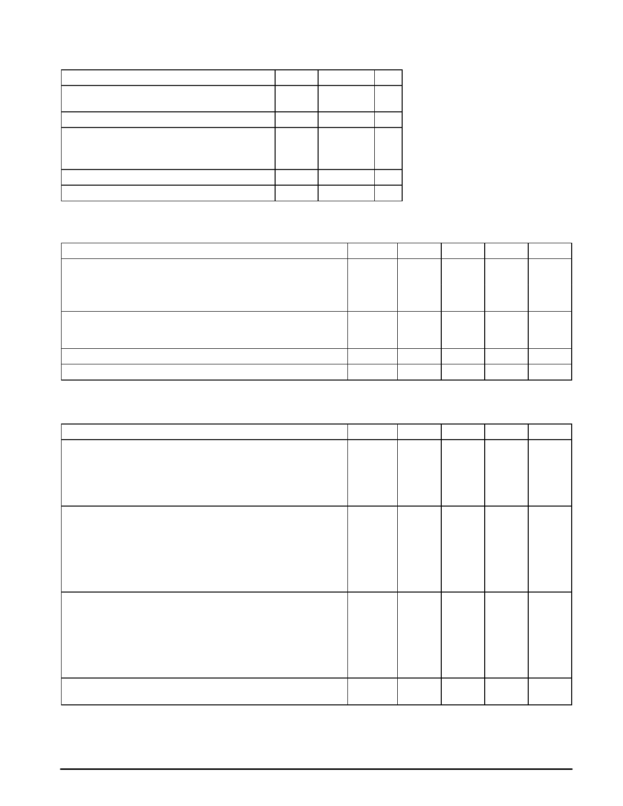
MAXIMUM OPERATING CONDITIONS (Pin numbers refer to DIP and SO–16
packages only.)
Rating
Symbol
Value
Unit
Power Supply Voltage
VCC
VEE
–0.5, +7.0 Vdc
–7.0, +0.5
Input Voltage (All Inputs)
Vin
Applied Output Voltage when in High Impedance Mode
Vza
(VCC = 5.0 V, Pin 4 = Logic 0, Pins 3, 6 = Logic 1)
–0.5, +20 Vdc
±15
Vdc
Output Voltage with VCC, VEE = 0 V
Output Current
Junction Temperature
Vzb
±15
IO
Self limiting –
TJ
–65, +150 °C
Devices should not be operated at these limits. The “Recommended Operating Conditions” table provides
conditions for actual device operation.
RECOMMENDED OPERATING CONDITIONS
Rating
Symbol
Min
Typ
Max
Unit
Power Supply Voltage (Differential Mode)
VCC
+4.75
5.0
+5.25
Vdc
VEE
–0.5
0
+0.3
Power Supply Voltage (Single–Ended Mode)
VCC
VEE
+4.75
+5.0
+5.25
–5.25
–5.0
–4.75
Input Voltage (All Inputs)
Applied Output Voltage (when in High Impedance Mode)
Applied Output Voltage, VCC = 0
Output Current
Operating Ambient Temperature (See text)
Vin
0
–
+15
Vdc
Vza
–10
–
+10
Vzb
–10
–
+10
IO
–65
–
+65
mA
TA
–40
–
+85
°C
All limits are not necessarily functional concurrently.
p t t p p ELECTRICAL CHARACTERISTICS (EIA–422–A differential mode, Pin 4 0.8 V, –40°C TA 85°C, 4.75 V VCC 5.25 V,
VEE = Gnd, unless otherwise noted. Pin numbers refer to DIP and SO–16 packages only.)
Characteristic
Symbol
Min
Typ
Max
Unit
Output Voltage (see Figure 1)
Differential, RL = ∞, VCC = 5.25 V
Differential, RL = 100 Ω, VCC = 4.75 V
Change in Differential Voltage, RL = 100 Ω (Note 4)
Offset Voltage, RL = 100 Ω
Change in Offset Voltage*, RL = 100 Ω
Output Current (each output)
p p Power Off Leakage, VCC = 0, –10 V VO +10 V
p p High Impedance Mode, VCC = 5.25 V, –10 V VO +10 V
Short Circuit Current (Note 2)
t t High Output Shorted to Pin 5 (TA = 25°C)
High Output Shorted to Pin 5 (–40°C TA +85°C)
t t Low Output Shorted to +6.0 V (TA = 25°C)
Low Output Shorted to +6.0 V (–40°C TA +85°C)
Inputs
Low Level Voltage
High Level Voltage
Current @ Vin = 2.4 V
Current @ Vin = 15 V
p p Current @ Vin = 0.4 V
Current, 0 Vin 15 V, VCC = 0
Clamp Voltage (Iin = –12 mA)
p p Power Supply Current (VCC = +5.25 V, Outputs Open)
(0 Enable VCC)
VOD1
–
4.2
6.0
Vdc
VOD2
2.0
2.6
–
Vdc
∆VOD2
–
10
400
mVdc
VOS
–
2.5
3.0
Vdc
∆VOS
–
10
400
mVdc
IOLK
–100
0
+100
µA
IOZ
–100
0
+100
ISC–
–150
–95
–60
mA
ISC–
–150
–
–50
ISC+
60
75
150
ISC+
50
–
150
VIL
–
–
0.8
Vdc
VIH
2.0
–
–
Vdc
IIH
–
0
40
µA
IIHH
–
0
100
IIL
–200
–8.0
–
IIX
–
0
–
VIK
–1.5
–
–
Vdc
ICC
mA
–
16
30
NOTES: 1. All voltages measured with respect to Pin 5.
2. Only one output shorted at a time, for not more than 1 second.
3. Typical values established at +25°C, VCC = +5.0 V, VEE = –5.0 V.
t u 4. Vin switched from 0.8 to 2.0 V.
5. Imbalance is the difference between VO2 with Vin 0.8 V and VO2 with Vin 2.0 V.
2
MOTOROLA ANALOG IC DEVICE DATA
Share Link: 