ADA4304-3ACPZ-R2(Rev0) 查看數據表(PDF) - Analog Devices
零件编号
产品描述 (功能)
生产厂家
ADA4304-3ACPZ-R2 Datasheet PDF : 12 Pages
| |||
ADA4304-3/ADA4304-4
ABSOLUTE MAXIMUM RATINGS
Table 2.
Parameter
Supply Voltage
Power Dissipation
Storage Temperature Range
Operating Temperature Range
Lead Temperature (Soldering, 10 sec)
Junction Temperature
Rating
5.5 V
See Figure 3
−65°C to +125°C
−40°C to +85°C
300°C
150°C
Stresses above those listed under Absolute Maximum
Ratings may cause permanent damage to the device. This is
a stress rating only; functional operation of the device at
these or any other conditions above those indicated in the
operational section of this specification is not implied.
Exposure to absolute maximum rating conditions for
extended periods may affect device reliability.
THERMAL RESISTANCE
θJA is specified for the device (including exposed pad)
soldered to a high thermal conductivity 4-layer (2s2p)
circuit board, as described in EIA/JESD 51-7.
Table 3. Thermal Resistance
Package Type
16-Lead LFCSP (Exposed Pad)
θJA
Unit
98
°C/W
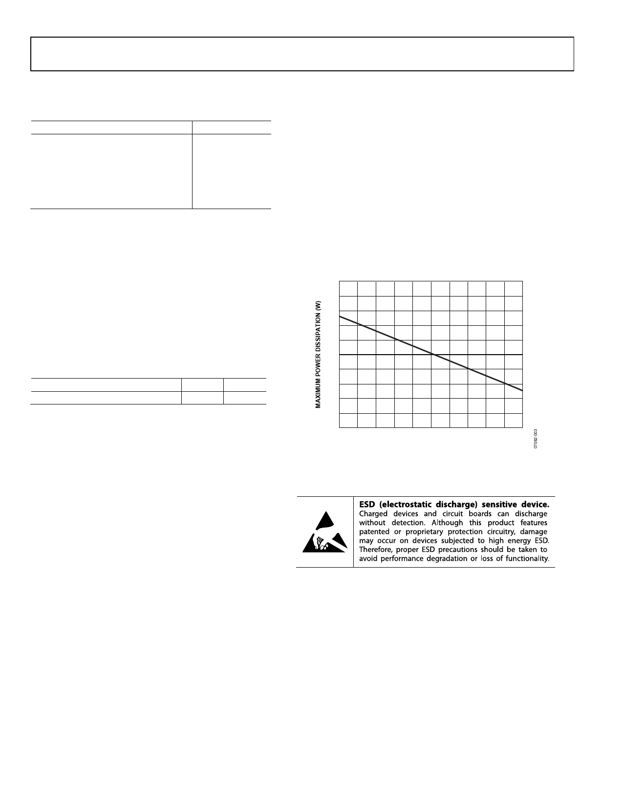
Maximum Power Dissipation
The maximum safe power dissipation in the ADA4304-3/
ADA4304-4 package is limited by the associated rise in
junction temperature (TJ) on the die. At approximately
150°C, which is the glass transition temperature, the plastic
changes its properties. Even temporarily exceeding this
temperature limit can change the stresses that the package
exerts on the die, permanently shifting the parametric
performance. Exceeding a junction temperature of 150°C
for an extended period can result in changes in the silicon
devices, potentially causing failure.
The power dissipated in the package (PD) is essentially equal to
the quiescent power dissipation, that is, the supply voltage (VS)
times the quiescent current (IS). In Table 1, the maximum
power dissipation of the ADA4304-3/ADA4304-4 can be
calculated as
PD (MAX) = 5.25 V × 105 mA = 551 mW
Airflow increases heat dissipation, effectively reducing θJA.
In addition, more metal directly in contact with the package
leads/exposed pad from metal traces, through-holes, ground,
and power planes reduces the θJA.
Figure 3 shows the maximum safe power dissipation in the
package vs. the ambient temperature for the 16-lead LFCSP
(98°C/W) on a JEDEC standard 4-layer board.
2.0
1.8
1.6
1.4
1.2
1.0
0.8
0.6
0.4
0.2
0
0 10 20 30 40 50 60 70 80 90 100
AMBIENT TEMPERATURE (°C)
Figure 3. Maximum Power Dissipation vs. Temperature for a 4-Layer Board
ESD CAUTION
Rev. 0 | Page 4 of 12
Share Link: 