BA10358F-E2(2009) 查看數據表(PDF) - ROHM Semiconductor
零件编号
产品描述 (功能)
生产厂家
BA10358F-E2
(Rev.:2009)
(Rev.:2009)
ROHM Semiconductor

BA10358F-E2 Datasheet PDF : 25 Pages
| |||
BA10358F/FV,BA10324AF/FV,BA2904SF/FV/FVM,BA2904F/FV/FVM,BA2904HFVM-C,
BA2902SF/FV/KN,BA2902F/FV/KN,BA3404F/FVM
Technical Note
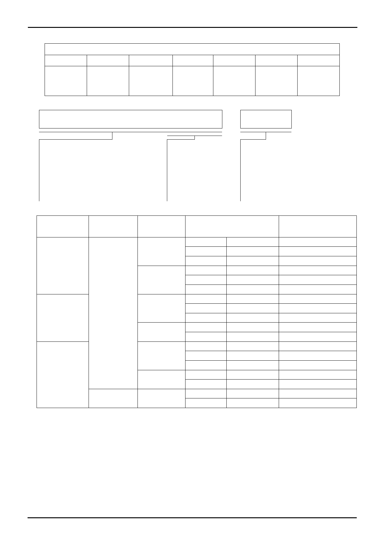
●Absolute Maximum Ratings (Ta=25[℃])
○BA2904S/BA2904/BA2902S/BA2902 family,BA2904HFVM-C
Parameter
Symbol
BA2904S family
BA2902S family
Rating
BA2904 family
BA2902 family
Supply Voltage
VCC-VEE
+32
Unit
BA2904HFVM-C
+36
V
Differential Input Voltage (*3)
Vid
32
36
V
Input Common-mode Voltage Range
Vicm
(VEE-0.3)~(VEE+32)
(VEE-0.3)~(VEE+36) V
Operating Temperature Range
Topr
-40~+105
-40~+125
℃
Storage Temperature Range
Tstg
-55~+150
℃
Maximum Junction Temperature
Tjmax
+150
℃
Note Absolute maximum rating item indicates the condition which must not be exceeded.
Application if voltage in excess of absolute maximum rating or use out of absolute maximum rated temperature environment may cause deterioration of characteristics.
(*3) The voltage difference between inverting input and non-inverting input is the differential input voltage. Then input terminal voltage is set to more than VEE.
●Electric Characteristics
○BA2904S/BA2904 family (Unless otherwise specified VCC=+5[V], VEE=0[V])
Parameter
Guaranteed limit
Symbol
Temperature
Range
BA2904S/BA2904 family
Unit
Min. Typ. Max.
Condition
Input Offset Voltage (*4)
Vio
25℃
Full range
-
-
2
-
7
10
mV
VOUT=1.4[V]
VCC=5~30[V],VOUT=1.4[V]
Input Offset Voltage Drift
△Vio/△T
-
±7
-
μV/℃ VOUT=1.4[V]
Input Offset Current (*4)
Iio
25℃
Full range
-
-
2
-
50
200
nA VOUT=1.4[V]
Input Offset Current Drift
△lio/△T
-
±10
-
pA/℃ VOUT=1.4[V]
Input Bias Current (*4)
Ib
25℃
Full range
-
-
20
-
250
250
nA VOUT=1.4[V]
Supply Current
Vicm
25℃
Full range
-
-
0.7
-
1.2
2
mA RL=∞All Op-Amps
25℃
3.5
-
High Level Output Voltage
VOH Full range
-
27
-
28
-
-
-
V RL=2[kΩ]
VCC=30[V],RL=10[kΩ]
Low Level
Output Voltage
VOL Full range
-
5
20
mV RL=∞All Op-Amps
Large Signal Voltage Gain
AV
25℃
25
100
-
V/mV
RL≧2[kΩ],VCC=15[V]
VOUT=1.4~11.4[V]
Input Common-mode
Voltage Range
Vicm
25℃
Full range
0
-
-
-
VCC-1.5
-
V
(VCC-VEE)=5V,VOUT=VEE+1.4[V]
Common-mode Rejection Ratio CMRR 25℃
50
80
-
dB VOUT=1.4[V]
Power Supply Rejection Ratio PSRR
25℃
65
100
-
dB VCC=5~30[V]
Output SourceCurrent (*5)
IOH
25℃
Full range
20
10
30
-
-
-
mA
VIN+=1[V],VIN-=0[V]
VOUT=0[V] 1CH is short circuit
Output Sink Current (*5)
IOL
25℃
Full range
10
2
20
-
Isink
25℃
12
40
-
-
mA
VIN+=0[V],VIN-=1[V]
VOUT=5[V] 1CH is short circuit
-
μA
VIN+=0[V],VIN-=1[V]
VOUT=200[mV]
Channel Separation
CS
25℃
-
120
-
dB f=1[kHz], input referred
Slew rate
SR
25℃
-
0.2
-
V/μs
VCC=15[V],AV=0[V],
RL=2[kΩ],CL=100[pF]
Maximum frequency
ft
25℃
-
0.5
-
MHz
VCC=30[V],RL=2[kΩ],
CL=100[pF]
Input referred noise voltage
Vn
25℃
-
40
-
nV/(Hz)1/2
VCC=15[V],VEE=-15[V],
RS=100[Ω],Vi=0[V],f=1[kHz]
(*4) Absolute value
(*5) Under high temperatures, please consider the power dissipation when selecting the output current.
When the output terminal is continuously shorted the output current reduces the internal temperature by flushing.
(*6) BA2904S family:Full range -40~105℃ BA2904 family:Full range -40~+125℃
www.rohm.com
© 2009 ROHM Co., Ltd. All rights reserved.
3/24
2009.05 - Rev.A
Share Link: