LTC4440 查看數據表(PDF) - Linear Technology
零件编号
产品描述 (功能)
生产厂家
LTC4440 Datasheet PDF : 14 Pages
| |||
LTC4440
Pin Functions
Exposed Pad MS8E Package
INP (Pin 1): Input Signal. TTL/CMOS compatible input
referenced to GND (Pin 2).
GND (Pins 2, 4): Chip Ground.
VCC (Pin 3): Chip Supply. This pin powers the internal low
side circuitry. A low ESR ceramic bypass capacitor should
be tied between this pin and the GND pin (Pin 2).
NC (Pin 5): No Connect. No connection required. For
convenience, this pin may be tied to Pin 6 (BOOST) on
the application board.
BOOST (Pin 6): High Side Bootstrapped Supply. An external
capacitor should be tied between this pin and TS (Pin 8).
Normally, a bootstrap diode is connected between VCC
(Pin 3) and this pin. Voltage swing at this pin is from VCC
– VD to VIN + VCC – VD, where VD is the forward voltage
drop of the bootstrap diode.
TG (Pin 7): High Current Gate Driver Output (Top Gate).
This pin swings between TS and BOOST.
TS (Pin 8): Top (High Side) Source Connection.
Exposed Pad (Pin 9): Ground. Must be electrically con-
nected to Pins 2 and 4 and soldered to PCB ground for
optimum thermal performance.
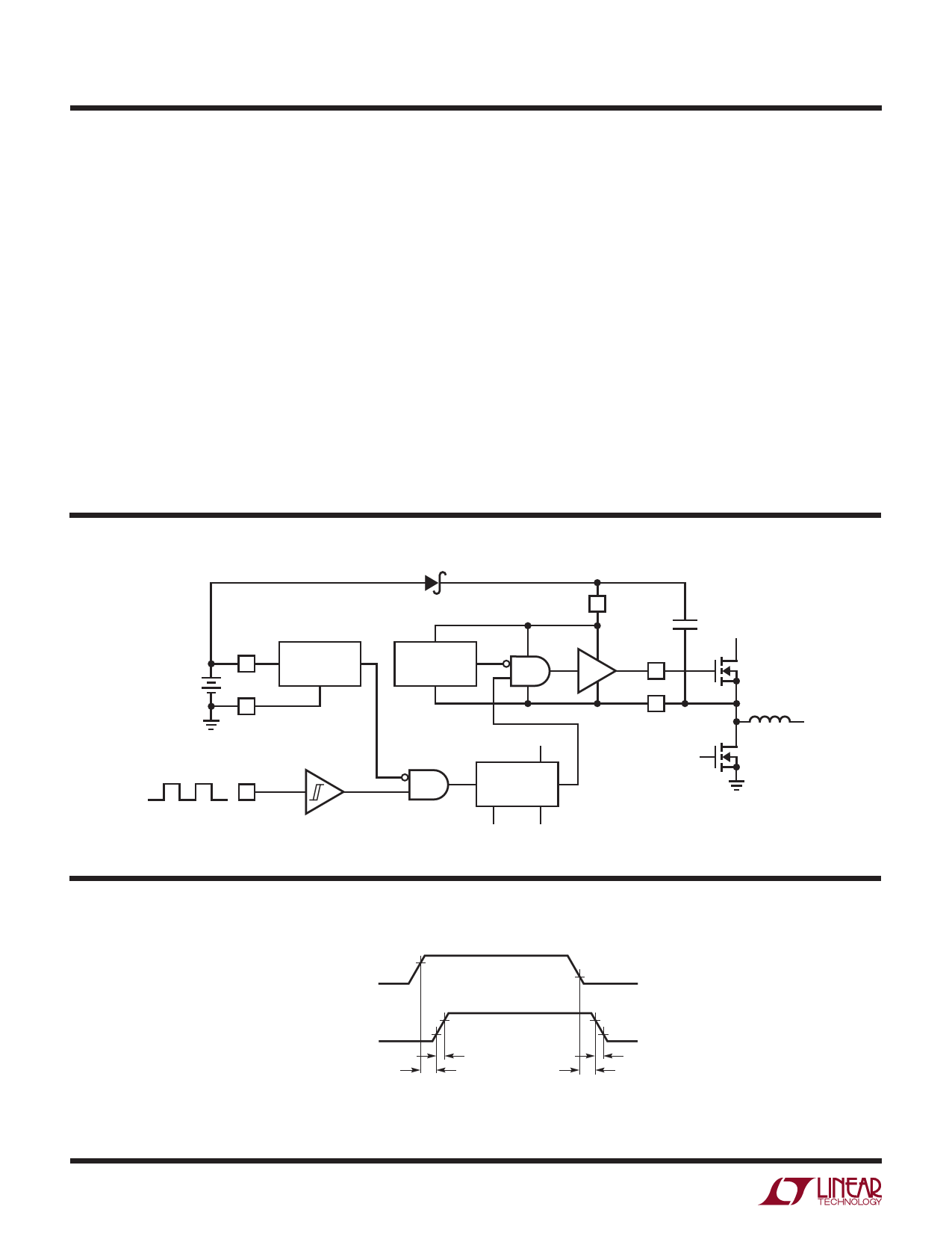
Block Diagram
8V TO 15V
VCC UNDERVOLTAGE
LOCKOUT
GND
INP
HIGH SIDE
UNDERVOLTAGE
LOCKOUT
BOOST
LEVEL SHIFTER
GND
TS
BOOST
TG
TS
VIN
UP TO 80V,
TRANSIENT
UP TO 100V
4440 BD
Timing Diagram
INPUT (INP)
OUTPUT (TG)
INPUT RISE/FALL TIME < 10ns
VIH
VIL
tr
tPLH
tf
tPHL
90%
10%
4440 TD
4440fa
6
For more information www.linear.com/LTC4440
Share Link: 