EL8172FSZ(2007) 查看數據表(PDF) - Intersil
零件编号
产品描述 (功能)
生产厂家
EL8172FSZ
(Rev.:2007)
(Rev.:2007)
Intersil

EL8172FSZ Datasheet PDF : 14 Pages
| |||
EL8171, EL8172
Description of Operation and Application
Information
Product Description
The EL8171 and EL8172 are micropower instrumentation
amplifiers (in-amps) which deliver rail-to-rail input amplification
and rail-to-rail output swing on a single 2.4V to 5.5V supply. The
EL8171 and EL8172 also deliver excellent DC and AC
specifications while consuming only 65µA typical supply
current. Because EL8171 and EL8172 provide an independent
pair of feedback terminals to set the gain and to adjust the
output level, these in-amps achieve high common-mode
rejection ratio regardless of the tolerance of the gain setting
resistors. The EL8171 is internally compensated for a minimum
closed loop gain of 10 or greater, well suited for moderate to
high gains. For higher gains, the EL8172 is internally
compensated for a minimum gain of 100. An EN pin is used to
reduce power consumption, typically 4.5µA, while the
instrumentation amplifier is disabled.
Input Protection
All input and feedback terminals of the EL8171 and EL8172
have internal ESD protection diodes to both positive and
negative supply rails, limiting the input voltage to within one
diode drop beyond the supply rails. The inverting inputs and
FB- inputs have ESD diodes to the V-rail, and the non-inverting
inputs and FB+ terminals have ESD diodes to the V+ rail. The
EL8172 has additional back-to-back diodes across the input
terminals and also across the feedback terminals. If overdriving
the inputs is necessary, the external input current must never
exceed 5mA. On the other hand, the EL8171 has no clamps to
limit the differential voltage on the input terminals allowing
higher differential input voltages at lower gain applications. It is
recommended however, that the input terminals of the EL8171
are not overdriven beyond 1V to avoid offset drift. An external
series resistor may be used as an external protection to limit
excessive external voltage and current from damaging the
inputs.
Input Stage and Input Voltage Range
The input terminals (IN+ and IN-) of the EL8171 and EL8172
are single differential pair P-MOSFET devices aided by an
Input Range Enhancement Circuit (IREC) to increase the
headroom of operation of the common-mode input voltage.
The feedback terminals (FB+ and FB-) also have a similar
topology. As a result, the input common-mode voltage range
of both the EL8171 and EL8172 is rail-to-rail. These in-amps
are able to handle input voltages that are at or slightly
beyond the supply and ground making these in-amps well
suited for single 5V or 3.3V low voltage supply systems.
There is no need to move the common-mode input of the in-
amps to achieve symmetrical input voltage.
Output Stage and Output Voltage Range
A pair of complementary MOSFET devices drive the output
VOUT to within a few mV of the supply rails. At a 100kΩ load,
the PMOS sources current and pulls the output up to 4mV
below the positive supply, while the NMOS sinks current and
pulls the output down to 4mV above the negative supply, or
ground in the case of a single supply operation. The current
sinking and sourcing capability of the EL8171 and EL8172
are internally limited to less than 35mA.
Gain Setting
VIN, the potential difference across IN+ and IN-, is replicated
(less the input offset voltage) across FB+ and FB-. The
obsession of the EL8171 and EL8172 in-amp is to maintain
the differential voltage across FB+ and FB- equal to IN+ and
IN-; (FB+ - FB-) = (IN+ - IN-). Consequently, the transfer
function can be derived. The gain of the EL8171 and EL8172
is set by two external resistors, the feedback resistor RF, and
the gain resistor RG.
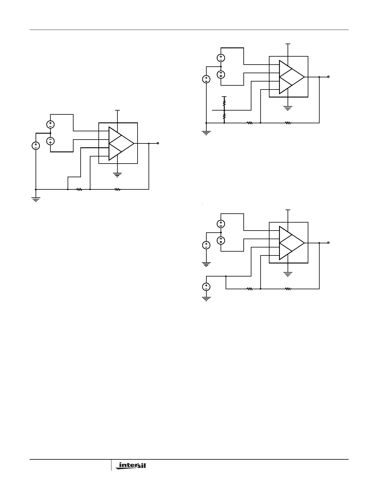
2.4V TO 5.5V
EN
VIN/2
VCM
VIN/2
71
2 IN+
V+ EN
+
3 IN-
-
6
8 FB+ EL8171/2
+
5 FB- -
V-
VOUT
4
RG
RF
FIGURE 39. CIRCUIT 1 - GAIN IS BY EXTERNAL RESISTORS
RF AND RG
VOUT
=
⎛
⎜
⎝
1
+
R-R----G-F--⎠⎟⎞
VIN
(EQ. 1)
In Figure 39, the FB+ pin and one end of resistor RG are
connected to GND. With this configuration, Equation 1 is
only true for a positive swing in VIN; negative input swings
will be ignored and the output will be at ground.
Reference Connection
Unlike a three-op amp instrumentation amplifier, a finite
series resistance seen at the REF terminal does not degrade
the EL8171 and EL8172's high CMRR performance,
eliminating the need for an additional external buffer
amplifier. Circuit 2 (Figure 40) uses the FB+ pin to provide a
high impedance REF terminal.
11
FN6293.3
August 3, 2007
Share Link: